
Pcb anatomy

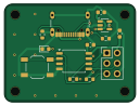
About the Pcb anatomy
Pcb anatomy is an open source AVR/Arduino PCB design by aguirrem, published on GitHub under the MIT license. It is a 2-layer board measuring 32 × 24 mm, with 13 components from 11 distinct parts.
Its main chip is the ATTINY85-20SU, from the AVR/Arduino family. Other key parts include the AP2112K-3.3TRG1. By type, the board carries 4 resistors, 3 capacitors, 2 ICs, 2 connectors, 1 switch and 1 diode.
From the project
An agent skill for hardware: design boards in KiCad, review them, and draw them. Modelled on Anatomy, whose isometric figure kit it builds on.
An agent skill for hardware: design boards in KiCad, review them, and draw them. Modelled on Anatomy, whose isometric figure kit it builds on.
examples/usb-blinky, drawn from its own .kicadpcb`: every part at its package height, the +3V3 net lit with current flowing along it.
Then in Claude Code: /pcb-anatomy design a breakout board for the BME280, I2C, 3.3 V, castellated edges. In the Claude app, upload the folder as a skill (zip it with SKILL.md at the root). Claude also picks the skill up whenever you ask for anything PCB, schematic, KiCad, Gerber or hardware-figure shaped.
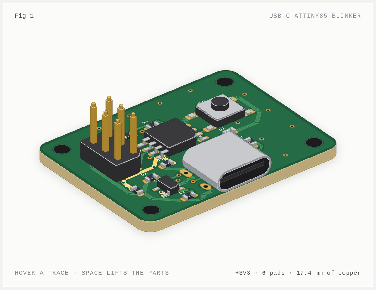
Main components on the Pcb anatomy
Pcb anatomy bill of materials (BOM)
13 components, 11 distinct parts — part numbers from the project's BOM.
| Qty | Part | Footprint | Refs |
|---|---|---|---|
| 1 | AP2112K-3.3TRG1 AP2112K-3.3 | SOT-23-5 | U1 |
| 1 | ATTINY85-20SU ATtiny85-20S | SOIC-8_5.3x5.3mm_P1.27mm | U2 |
| 1 | USB4105-GF-A | USB_C_Receptacle_GCT_USB4105-xx-A_16P_TopMnt_Horizontal | J1 |
| 1 | ISP | PinHeader_2x03_P2.54mm_Vertical | J2 |
| 1 | TL3342 | SW_SPST_TL3342 | SW1 |
| 1 | green | LED_0603_1608Metric | D1 |
| 2 | 1u | C_0603_1608Metric | C1, C2 |
| 1 | 100N 100n | C_0603_1608Metric | C3 |
| 2 | 5.1K 5.1k | R_0603_1608Metric | R1, R2 |
| 1 | 10K 10k | R_0603_1608Metric | R3 |
| 1 | 330 | R_0603_1608Metric | R4 |
Pcb anatomy design files
The KiCad project lives in the aguirrem/pcb-anatomy repository on GitHub; these links point at the commit this page was built from.
Pcb anatomy: common questions
What microcontroller does the Pcb anatomy use?
The Pcb anatomy is built around the ATTINY85-20SU, from the AVR/Arduino family.
How big is the Pcb anatomy?
The Pcb anatomy measures 32 × 24 mm, has 2 copper layers and is 1.6 mm thick.
How many components are on the Pcb anatomy?
13 components, from 11 distinct parts, with part numbers taken from the project's own BOM. The full bill of materials is listed on this page.
Where can I download the Pcb anatomy design files?
From the aguirrem/pcb-anatomy repository on GitHub, which has the KiCad layout, the schematic and the BOM; the links under Design files point to each one.
Can I use the Pcb anatomy design in my own project?
Yes, under the terms of its MIT license, which aguirrem chose for the repository.
Can I test firmware for the Pcb anatomy without the hardware?
Yes. HardLabs builds a simulation of the board from its netlist and BOM, so you can run and debug AVR/Arduino firmware against it before you order a PCB.
Similar boards
 AVR/Arduino
Magspoof
samyk
35 × 29 mm11 parts2LNo license4.2k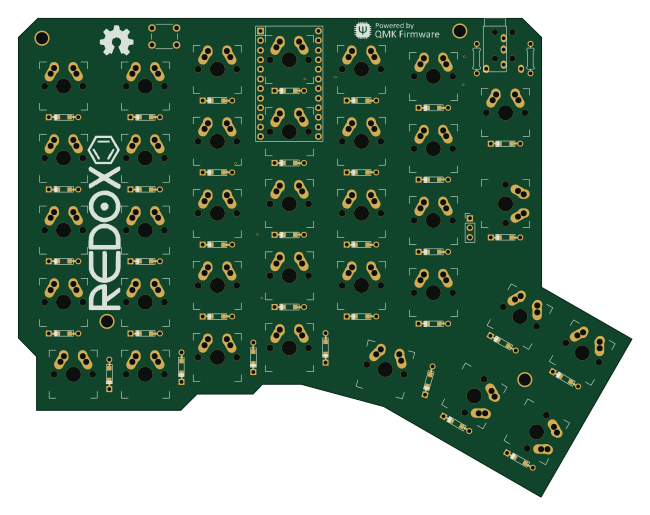 AVR/Arduino
Redox keyboard
mattdibi
162.2 × 126.5 mm77 parts2LMIT2.0k AVR/Arduino
Labrador
espotek-org
36.8 × 34.7 mm75 parts2LNo license1.2k AVR/Arduino
V4
stuartpittaway
30 × 50 mm38 parts2LCC-BY-NC-4.01.1k AVR/Arduino
ModuleV450
30 × 61.4 mm39 parts2LCC-BY-NC-4.01.1k AVR/Arduino
Discipline
coseyfannitutti
304.9 × 122.8 mm170 parts2LCC-BY-NC-4.01.0k