
MAIN V1.2

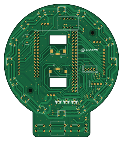
About the MAIN V1.2 PCB
MAIN V1.2 is an open source AVR/Arduino PCB design by akihiro-kataoka, published on GitHub. It is a 2-layer board measuring 100 × 115 mm, with 67 components from 20 distinct parts.
Its main chip is the Mega 2560 ProMini footprint, from the AVR/Arduino family. By type, the board carries 20 capacitors, 16 diodes, 11 resistors, 4 transistors, 1 IC and 1 buzzer.
Main components on the MAIN V1.2
MAIN V1.2 bill of materials (BOM)
67 components, 20 distinct parts — part numbers from the project's BOM.
| Qty | Part | Footprint | Refs |
|---|---|---|---|
| 1 | Mega 2560 ProMini footprint | ARDUINO_MEGA_2560_PRO | U1 |
| 4 | BSS138 | SOT-23 | Q1, Q2, Q3, Q4 |
| 1 | CONN_01X08_PIN Conn_01x08_Pin | BNO055 | BNO55 |
| 1 | Buzzer | Buzzer UDX01CLFPH | BZ1 |
| 2 | Conn_01x09_Pin | PinSocket_1x09_P2.54mm_Vertical | Ball-D15.17.19.23.25.27.29.31, Ball-D32.34.36.38.40.42.44.46 |
| 2 | Conn_01x04_Pin | JST_XH_B4B-XH-A_1x04_P2.50mm_Vertical | CAM1, CAM2 |
| 3 | Conn_01x03_Pin | JST_XH_B3B-XH-A_1x03_P2.50mm_Vertical | Catch1, Catch2, 電源1 |
| 1 | Conn_01x06_Pin | CON_522710679_MOL | LINE-A9.11.13,D22.24.26 |
| 1 | Conn_01x08_Pin | CON_522710879_MOL | MOTOR-D2.3.4.5.6.7.8.9 |
| 2 | SW_Push | SW_PUSH_6mm | TactSwitch1, TactSwitch3 |
| 1 | SW_Push | SW_TL1100EF160Q | TactSwitch2 |
| 1 | Conn_01x03_Pin | PinSocket_1x03_P2.54mm_Vertical | ToggleSwitch1 |
| 16 | WS2812B | LED_WS2812B_PLCC4_5.0x5.0mm_P3.2mm | D1, D2, D3, D4, D5, D6, D7, D8 +8 |
| 1 | 100μF | CP_Radial_D5.0mm_P2.50mm | C1 |
| 1 | 47μF | CP_Radial_D5.0mm_P2.50mm | C2 |
| 1 | 0.1μF | CP_Radial_D5.0mm_P2.50mm | C3 |
| 17 | 0.1μF | C_0603_1608Metric_Pad1.08x0.95mm_HandSolder | C4, C5, C6, C7, C8, C9, C10, C11 +9 |
| 1 | 1kΩ | R_0805_2012Metric_Pad1.20x1.40mm_HandSolder | R1 |
| 2 | 3.3kΩ | R_0805_2012Metric_Pad1.20x1.40mm_HandSolder | R2, R3 |
| 8 | 10kΩ | R_0603_1608Metric | R4, R5, R6, R7, R8, R9, R10, R11 |
MAIN V1.2 design files
The KiCad project lives in the akihiro-kataoka/KiCad_Circuit-Board_data repository on GitHub; these links point at the commit this page was built from.
MAIN V1.2: common questions
What microcontroller does the MAIN V1.2 use?
The MAIN V1.2 is built around the Mega 2560 ProMini footprint, from the AVR/Arduino family.
How big is the MAIN V1.2 PCB?
The MAIN V1.2 measures 100 × 115 mm, has 2 copper layers and is 1.6 mm thick.
How many components are on the MAIN V1.2?
67 components, from 20 distinct parts, with part numbers taken from the project's own BOM. The full bill of materials is listed on this page.
Where can I download the MAIN V1.2 design files?
From the akihiro-kataoka/KiCad_Circuit-Board_data repository on GitHub, which has the KiCad layout, the schematic and the BOM; the links under Design files point to each one.
Can I use the MAIN V1.2 design in my own project?
The repository has no license, so all rights stay with akihiro-kataoka. Use it as a reference, and ask the author before reusing the design.
Can I test firmware for the MAIN V1.2 without the hardware?
Yes. HardLabs builds a simulation of the board from its netlist and BOM, so you can run and debug AVR/Arduino firmware against it before you order a PCB.
More boards in KiCad_Circuit-Board_data
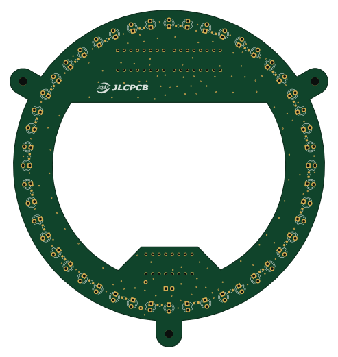
LINESensorV4.1
122.6 × 130 mm78 parts2LNo license0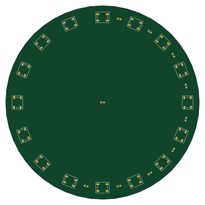
NeoPixel
100 × 100 mm34 parts2LNo license0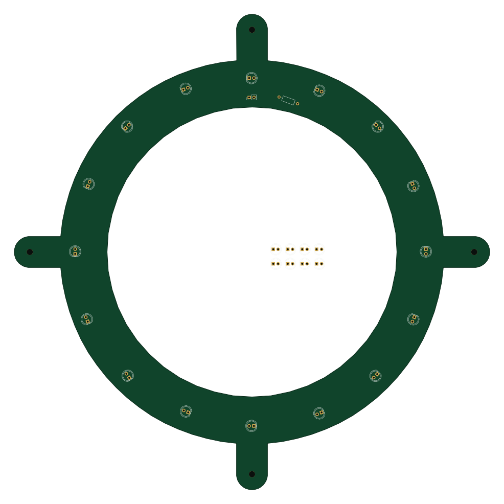
Enjoy!!!
246 × 246 mm26 parts2LNo license0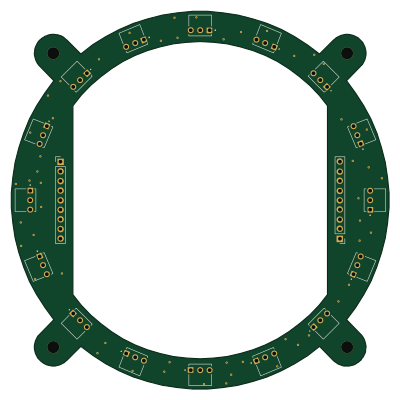
BALLSensorV2.1
99.9 × 99.9 mm18 parts2LNo license0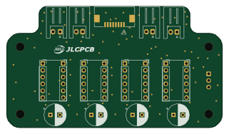
MOTORDRIVEV2.1
80 × 45 mm14 parts2LNo license0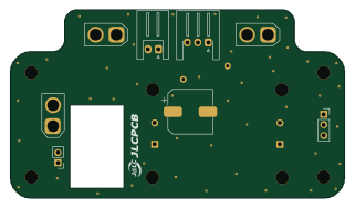
ELECT V2.1
80 × 45 mm10 parts2LNo license0
Ballcatch sensor
28 × 10 mm4 parts2LNo license0
YoutubeStudy
47 × 29 mm3 parts2LNo license0
LEDtentou
50 × 35 mm3 parts2LNo license0
Earlier revisions in the repo: MAIN V1.1
Similar boards
 AVR/Arduino
V4
stuartpittaway
30 × 50 mm38 parts2LCC-BY-NC-4.01.1k AVR/Arduino
ModuleV450
30 × 61.4 mm39 parts2LCC-BY-NC-4.01.1k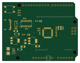 AVR/Arduino
Easyduino Atmega
Hanqaqa
68.8 × 53.6 mm35 parts4LCERN-OHL-P-2.0746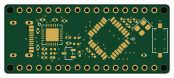 AVR/Arduino
Easyduino Atmega Nano
43.4 × 18 mm30 parts4LCERN-OHL-P-2.0746 AVR/Arduino
UsbGpib
xyphro
54 × 15 mm21 parts2LMIT683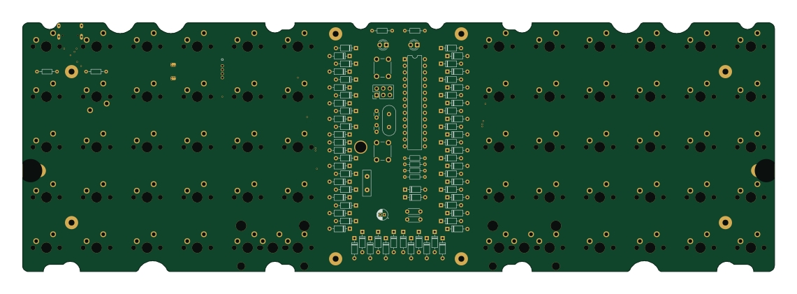 AVR/Arduino
Lumberjack
peej
284.7 × 94.2 mm149 parts2LMIT402