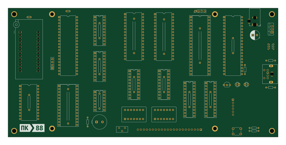
Main

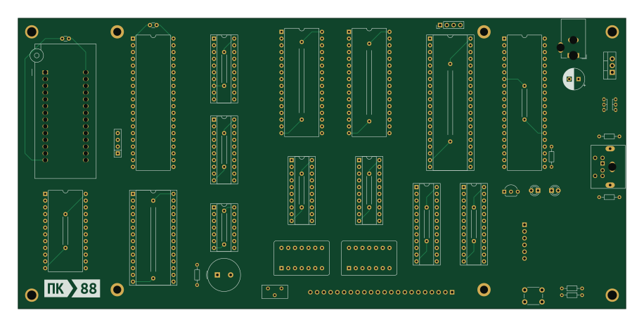
About the Main PCB
Main is an open source PCB design by and3rson, published on GitHub under the MIT license. It is a 2-layer board measuring 228.6 × 109.2 mm, with 57 components from 35 distinct parts.
Other key parts include the L7805, 74HC14 and DS1813-5+. By type, the board carries 16 capacitors, 7 resistors, 3 ICs, 3 connectors, 2 crystals and 2 switches.
From the project
Single-board computer based on KM1810VM88 CPU (Ukrainian clone of Intel 8088).
Single-board computer based on KM1810VM88 CPU (Ukrainian clone of Intel 8088) that can run ELKS!
PK stands for Персональний Комп'ютер ("Personalnii Kompyuter", i.e. "Personal Computer") in Ukrainian.
This board runs @ 8 MHz (24 MHz oscillator) in minimum mode.
- KiCad schematics - GAL sources - Address & I/O port decoders using 2x ATF16V8 - Various circuit simulations - made with Digital - MetalBIOS - IBM PC XT compatible-ish BIOS that I made specifically for PK-88
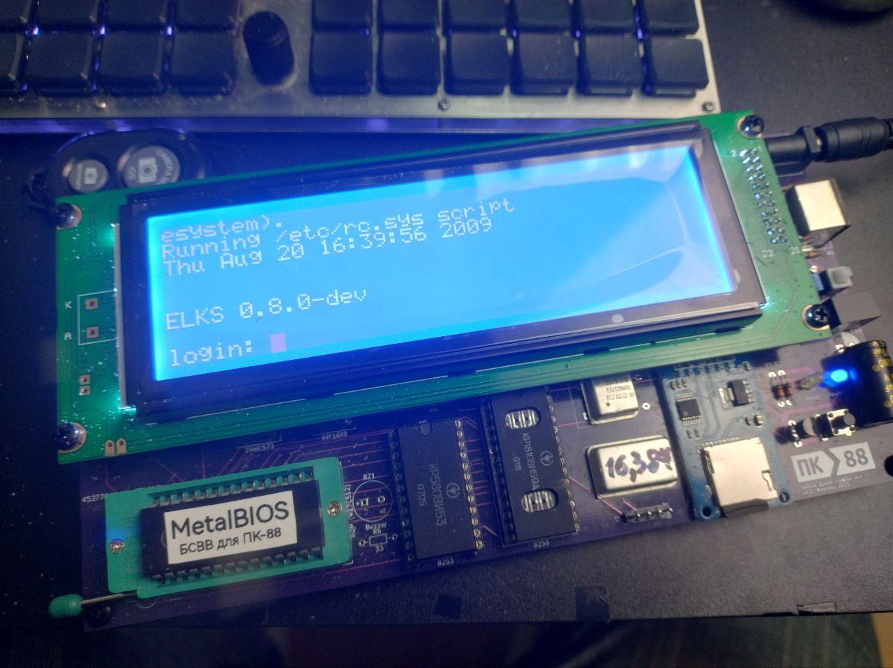
Main components on the Main
Main bill of materials (BOM)
57 components, 35 distinct parts.
| Qty | Part | Footprint | Refs |
|---|---|---|---|
| 1 | L7805 | TO-220-3_Vertical | U1 |
| 1 | 74HC14 | DIP-14_W7.62mm_Socket | U2 |
| 1 | DS1813-5+ | TO-92L_Inline_Wide | U3 |
| 1 | 15 MHz | Oscillator_DIP-8-14 | X1 |
| 1 | 1.8432 MHz | Oscillator_DIP-8-14 | X2 |
| 1 | Barrel_Jack | BarrelJack_Wuerth_6941xx301002 | J1 |
| 1 | UART | PinHeader_1x04_P2.54mm_Vertical | J2 |
| 1 | Mini-DIN_6pins_ver3 | Connector_Mini-DIN_Female_6Pin_2rows | P1 |
| 2 | 74HC573 | DIP-20_W7.62mm_Socket | ADDR1, ADDR2 |
| 1 | Buzzer | Buzzer_TDK_PS1240P02BT_D12.2mm_H6.5mm | BZ1 |
| 1 | KM1810VM88 | DIP-40_W15.24mm | CPU1 |
| 2 | ATF16V8 | DIP-20_W7.62mm_Socket | DEC1, DEC2 |
| 4 | MountingHole | Hole_3.5x5 | H1, H2, H3, H4 |
| 1 | ATF22V10 | DIP-24_W7.62mm_Socket | KB1 |
| 1 | T6963C | LCD240128_TFT_var2 | LCD1 |
| 1 | 8259 | DIP-28_W15.24mm_Socket | PIC1 |
| 1 | 8253 | DIP-24_W15.24mm | PIT1 |
| 1 | 8255 | DIP-40_W15.24mm | PPI1 |
| 1 | RAM1 (AS6C4008) | DIP-32_W15.24mm | RAM1 |
| 1 | RAM2 (AS6C4008) | DIP-32_W15.24mm | RAM2 |
Show 15 more
| Qty | Part | Footprint | Refs |
|---|---|---|---|
| 1 | ROM (W27C512) | ZIF28 | ROM1 |
| 1 | R_Potentiometer | Potentiometer_Bourns_3296Y_Vertical | RV1 |
| 1 | uSD adapter | MicroSD-Adapter | SD1 |
| 1 | ATF750C_SPI | DIP-24_W7.62mm_Socket | SPI1 |
| 1 | Reset | SW_PUSH_6mm_H5mm | SW1 |
| 1 | SW_Push_DPDT | PB22E06 | SW2 |
| 1 | 16550 | DIP-40_W15.24mm_Socket | UART1 |
| 1 | Power | LED_D3.0mm | D1 |
| 1 | Reset | LED_D3.0mm | D2 |
| 9 | 0.1 uF | C_Disc_Long | C1, C2, C4, C5, C7, C8, C10, C15 +1 |
| 2 | 0.1 uF | C_Disc_D3.0mm_W1.6mm_P2.50mm | C3, C11 |
| 4 | 0.1 uF | C_Disc_VeryLong | C6, C9, C12, C13 |
| 1 | 10 uF | CP_Radial_D8.0mm_P3.50mm | C14 |
| 6 | 10K | R_Axial_DIN0204_L3.6mm_D1.6mm_P7.62mm_Horizontal | R1, R2, R3, R4, R5, R6 |
| 1 | R_Network03_Split | R_Array_SIP4 | RN1 |
Main design files
The KiCad project lives in the and3rson/pk88 repository on GitHub; these links point at the commit this page was built from.
- Layoutkicad/main.kicad_pcb
- Schematickicad/main.kicad_sch
Main: common questions
How big is the Main PCB?
The Main measures 228.6 × 109.2 mm, has 2 copper layers and is 1.6 mm thick.
How many components are on the Main?
57 components, from 35 distinct parts. The full bill of materials is listed on this page.
Where can I download the Main design files?
From the and3rson/pk88 repository on GitHub, which has the KiCad layout and the schematic; the links under Design files point to each one.
Can I use the Main design in my own project?
Yes, under the terms of its MIT license, which and3rson chose for the repository.