
D11-nano dbg


About the D11-nano dbg PCB
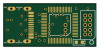
D11-nano dbg is an open source Microchip SAM PCB design by ataradov, published on GitHub under the BSD-3-Clause license. It is a 2-layer board measuring 15.2 × 10.9 mm, with 13 components from 11 distinct parts.
Its main chip is the ATSAMD11C, from the Microchip SAM family. Other key parts include the SC662K-3.3. By type, the board carries 3 test points, 3 resistors, 2 ICs, 2 connectors, 2 capacitors and 1 LED.
It belongs with the usb & debug tools designs in this gallery.
From the project
Free and open implementation of the CMSIS-DAP debugger firmware
This is a free and open implementation of the CMSIS-DAP debugger firmware.
Both SWD and JTAG protocols are supported. However JTAG was not well tested due to lack of good targets. If you have any issues with it - let me know and I'll try to help.
To create a CMSIS-DAP compliant debugger, your platform must: Implement USB HID (and raw bulk for CMSIS-DAP v2) device able to receive and send arbitrary payloads Provide configuration file dapconfig.h with definitions for hardware-dependent calls Call dapinit() at the initialization time Call dapprocessrequest() for every received request and send…
Main components on the D11-nano dbg
D11-nano dbg bill of materials (BOM)
13 components, 11 distinct parts.
| Qty | Part | Footprint | Refs |
|---|---|---|---|
| 1 | SC662K-3.3 | SOT-23 | IC1 |
| 1 | ATSAMD11C | SOIC-14 | IC2 |
| 1 | USB-C | USB-C | J1 |
| 1 | Conn-5x2 | Header-5x2-1.27mm-SMD | J2 |
| 1 | SCK | TestPoint-1.27mm-SMD | TP1 |
| 1 | RST | TestPoint-1.27mm-SMD | TP2 |
| 1 | SIO | TestPoint-1.27mm-SMD | TP3 |
| 1 | Orange | 0603 | LED1 |
| 2 | 1uF | 0603 | C1, C2 |
| 2 | 5.1K | 0603 | R1, R2 |
| 1 | 20K | 0603 | R3 |
D11-nano dbg design files
The KiCad project lives in the ataradov/free-dap repository on GitHub; these links point at the commit this page was built from.
D11-nano dbg: common questions
What microcontroller does the D11-nano dbg use?
The D11-nano dbg is built around the ATSAMD11C, from the Microchip SAM family.
How big is the D11-nano dbg PCB?
The D11-nano dbg measures 15.2 × 10.9 mm, has 2 copper layers and is 1.6 mm thick.
How many components are on the D11-nano dbg?
13 components, from 11 distinct parts. The full bill of materials is listed on this page.
Where can I download the D11-nano dbg design files?
From the ataradov/free-dap repository on GitHub, which has the KiCad layout and the schematic; the links under Design files point to each one.
Can I use the D11-nano dbg design in my own project?
Yes, under the terms of its BSD-3-Clause license, which ataradov chose for the repository.
Can I test firmware for the D11-nano dbg without the hardware?
Yes. HardLabs builds a simulation of the board from its netlist and BOM, so you can run and debug Microchip SAM firmware against it before you order a PCB.
More boards in free-dap
Similar boards
 Microchip SAM
Microcontroller Expansion Card
FrameworkComputer
26 × 30 mm24 parts2LCC-BY-4.01.1k Microchip SAM
Taco Raven
VoronDesign
120 × 113 mm349 parts4LGPL-3.01.1k Microchip SAM
Fpgaboy
Wren6991
50 × 50 mm89 parts4LNo license508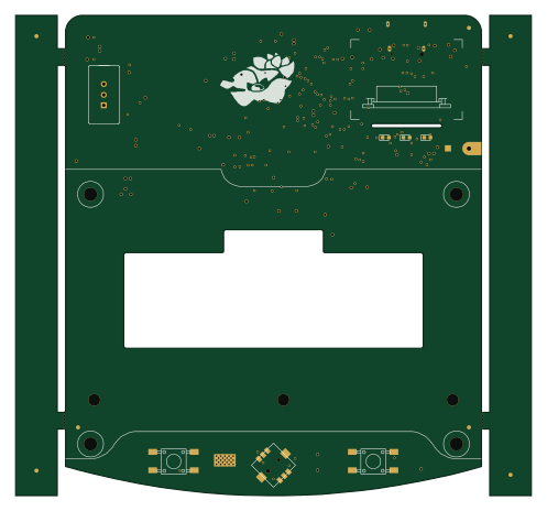 Microchip SAM
OpenDropV4
GaudiLabs
124 × 115.4 mm118 parts2LGPL-3.0487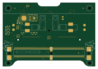 Microchip SAM
ModulAdapter universal
100 × 69.5 mm45 parts2LGPL-3.0487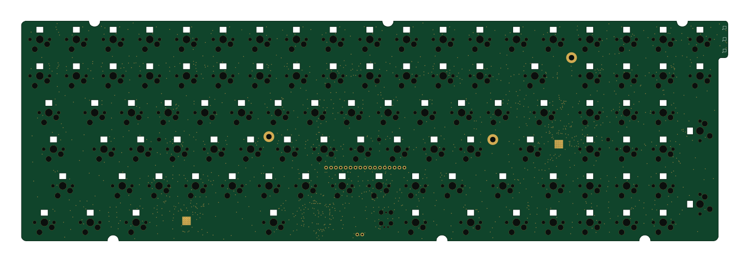 Microchip SAM
Kira
kiibohd
366.9 × 114.3 mm400 partsCERN-OHL-1.2415