
Nand pcb test

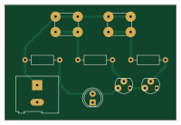
About the Nand pcb test
Nand pcb test is an open source PCB design by barrettotte, published on GitHub under the MIT license. It is a 2-layer board measuring 50 × 33.5 mm, with 9 components from 6 distinct parts.
By type, the board carries 3 resistors, 2 transistors, 2 switches, 1 connector and 1 diode.
It belongs with the robotics & motion designs in this gallery.
From the project
Homemade PCB test using a CNC router
Hopefully this is useful to someone else wanting a single place to see the whole CNC PCB building process. These notes assume you have a basic understanding of Kicad and Candle (grblcontrol).
There are plenty of companies that offer cheap PCB manufacturing, but I'm impatient and bad at designing things correctly on the first try. Imagine ordering a PCB, waiting a few days, and figuring out you messed up your design. Manufacturing with a CNC router helps to eliminate waiting time between idea and implementation.
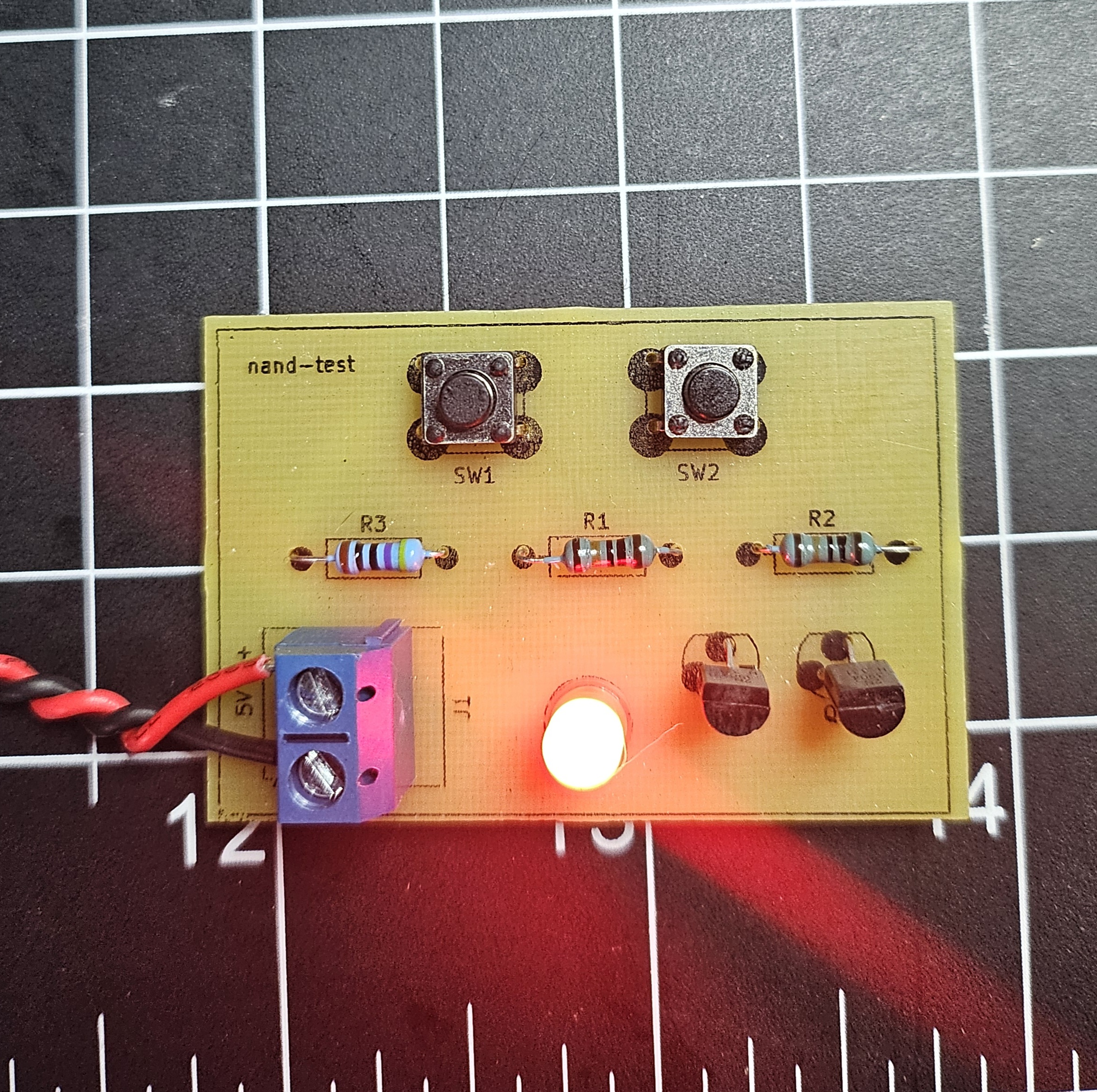
Nand pcb test bill of materials (BOM)
9 components, 6 distinct parts.
| Qty | Part | Footprint | Refs |
|---|---|---|---|
| 2 | 2N3904 | TO-92_Inline | Q1, Q2 |
| 1 | PWR | TerminalBlock_Altech_AK300-2_P5.00mm | J1 |
| 2 | SW_SPST | SW_PUSH_6mm | SW1, SW2 |
| 1 | LED | LED_D5.0mm | D1 |
| 2 | 10K | R_Axial_DIN0207_L6.3mm_D2.5mm_P10.16mm_Horizontal | R1, R2 |
| 1 | 470 | R_Axial_DIN0207_L6.3mm_D2.5mm_P10.16mm_Horizontal | R3 |
Nand pcb test design files
The KiCad project lives in the barrettotte/nand-pcb-test repository on GitHub; these links point at the commit this page was built from.
- Layoutkicad/nand-test.kicad_pcb
- Schematickicad/nand-test.kicad_sch
Nand pcb test: common questions
How big is the Nand pcb test?
The Nand pcb test measures 50 × 33.5 mm, has 2 copper layers and is 1.6 mm thick.
How many components are on the Nand pcb test?
9 components, from 6 distinct parts. The full bill of materials is listed on this page.
Where can I download the Nand pcb test design files?
From the barrettotte/nand-pcb-test repository on GitHub, which has the KiCad layout and the schematic; the links under Design files point to each one.
Can I use the Nand pcb test design in my own project?
Yes, under the terms of its MIT license, which barrettotte chose for the repository.
Similar boards

Stack chan
stack-chan
50 × 50 mm33 parts2LApache-2.01.7k
Cube batteryboard
willem-pennings
95 × 95 mm4 parts2LGPL-3.01.1k
Mesabob
rene-dev
87.5 × 50 mm44 parts2LGPL-3.0979
Bob
100 × 100 mm140 parts2LGPL-3.0979
Triple adapter
57 × 75 mm26 parts2LGPL-3.0979
Trollerv2
100 × 75 mm33 parts4LGPL-3.0979