
HATB ver 8

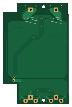
About the HATB ver 8 PCB
HATB ver 8 is an open source PCB design by ConnectBox, published on GitHub. It is a 2-layer board measuring 57.6 × 88.2 mm, with 21 components from 12 distinct parts.
By type, the board carries 8 resistors, 4 transistors, 4 diodes, 2 battery holders, 2 capacitors and 1 connector.
From the project
Connectbox Circuit Design
This repo contains the schematic and KiCAD design files for the NEO-USB-HAT. This is a daugherboard to add an extra USB port and power input to a NanoPi NEO.
HATB ver 8 bill of materials (BOM)
21 components, 12 distinct parts — part numbers from the project's BOM.
| Qty | Part | Footprint | Refs |
|---|---|---|---|
| 2 | 3J15 Toshiba | SOT-323_SC-70 | Q1, Q3 |
| 2 | 8205A | TSSOP-8_4.4x3mm_P0.65mm | Q2, Q4 |
| 1 | Conn_01x02_Female | PinSocket_1x02_P2.54mm_Vertical | P10 |
| 2 | Battery_multi_cell | Battery 21700 | BT1, BT2 |
| 4 | MMBD914 ON Semiconductor | D_SOT-23_ANK | D4, D5, D6, D7 |
| 2 | 1uF KEMET | C_0805_2012Metric | C19, C20 |
| 2 | 100K Yageo | R_0603_1608Metric | R21, R25 |
| 1 | RC0805FR-071KL 100K Yageo | R_0603_1608Metric | R22 |
| 1 | 20K Yageo | R_0603_1608Metric | R23 |
| 2 | 10K Yageo | R_0603_1608Metric | R24, R28 |
| 1 | RC0805FR-07200KL 100K Yageo | R_0603_1608Metric | R26 |
| 1 | RC0805FR-0727KL 20K Yageo | R_0603_1608Metric | R27 |
HATB ver 8 design files
The KiCad project lives in the ConnectBox/Circuit-Design repository on GitHub; these links point at the commit this page was built from.
HATB ver 8: common questions
How big is the HATB ver 8 PCB?
The HATB ver 8 measures 57.6 × 88.2 mm, has 2 copper layers and is 1.6 mm thick.
How many components are on the HATB ver 8?
21 components, from 12 distinct parts, with part numbers taken from the project's own BOM. The full bill of materials is listed on this page.
Where can I download the HATB ver 8 design files?
From the ConnectBox/Circuit-Design repository on GitHub, which has the KiCad layout, the schematic and the BOM; the links under Design files point to each one.
Can I use the HATB ver 8 design in my own project?
The repository has no license, so all rights stay with ConnectBox. Use it as a reference, and ask the author before reusing the design.
More boards in Circuit-Design
 AVR/Arduino
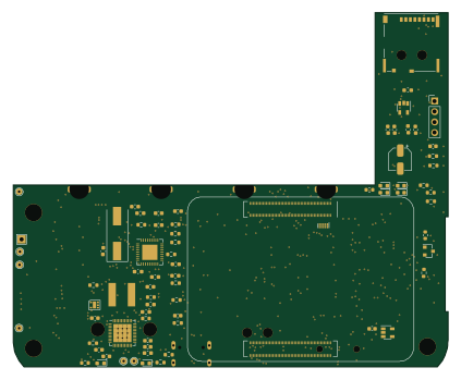
HAT CM4 183
105.6 × 86.1 mm161 parts6LNo license0 AVR/Arduino
HAT CM4 DRC 1
105.6 × 86.1 mm147 parts6LNo license0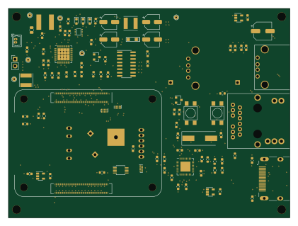 AVR/Arduino
ConnectBox HAT using RPi CM4
105 × 78 mm130 parts4LNo license0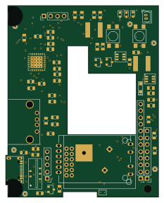
HAT ver 7
57.4 × 71.6 mm72 parts2LNo license0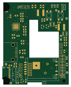
HAT ver 8
57.4 × 71.6 mm72 parts2LNo license0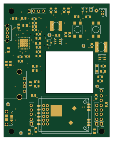
HAT ver 6.0
56.6 × 71.6 mm68 parts2LNo license0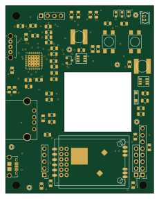
HAT ver 5.1
56.6 × 71.6 mm68 parts2LNo license0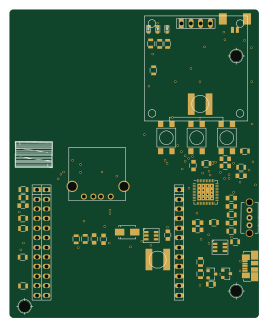
NanoPi NEO USB HAT - Version 4.7
66 × 81.6 mm63 parts2LNo license0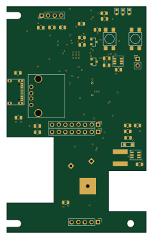
ConnectBox HAT 8
53.7 × 87 mm60 parts4LNo license0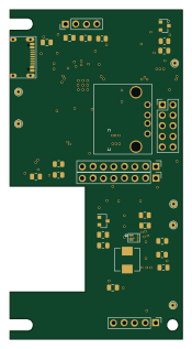
ConnectBox HAT-A
41.6 × 79.2 mm54 parts4LNo license0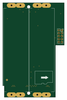
ConnectBox - Battery Board
52.3 × 80.4 mm31 parts2LNo license0