
Full wave rectifier

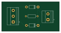
About the Full wave rectifier PCB
Full wave rectifier is an open source PCB design by Constellation-destroyer, published on GitHub under the MIT license. It is a 2-layer board measuring 50 × 25.5 mm, with 5 components from 4 distinct parts.
By type, the board carries 2 connectors, 2 diodes and 1 resistor.
It belongs with the iot & wireless and sensors designs in this gallery.
From the project
KiCad PCB designs from my IoT Research Internship includes analog circuits, IoT sensor boards, and multi-sensor health monitoring system.
Full wave rectifier bill of materials (BOM)
5 components, 4 distinct parts.
| Qty | Part | Footprint | Refs |
|---|---|---|---|
| 1 | Input | TerminalBlock_Phoenix_MKDS-1,5-3_1x03_P5.00mm_Horizontal | J1 |
| 1 | Output | TerminalBlock_Phoenix_MKDS-1,5-2_1x02_P5.00mm_Horizontal | J2 |
| 2 | 1N4007 | D_DO-41_SOD81_P10.16mm_Horizontal | D1, D2 |
| 1 | 1.2K | R_Axial_DIN0207_L6.3mm_D2.5mm_P10.16mm_Horizontal | R1 |
Full wave rectifier design files
The KiCad project lives in the Constellation-destroyer/PCB-design-in-KiCad9.0 repository on GitHub; these links point at the commit this page was built from.
Full wave rectifier: common questions
How big is the Full wave rectifier PCB?
The Full wave rectifier measures 50 × 25.5 mm, has 2 copper layers and is 1.6 mm thick.
How many components are on the Full wave rectifier?
5 components, from 4 distinct parts. The full bill of materials is listed on this page.
Where can I download the Full wave rectifier design files?
From the Constellation-destroyer/PCB-design-in-KiCad9.0 repository on GitHub, which has the KiCad layout and the schematic; the links under Design files point to each one.
Can I use the Full wave rectifier design in my own project?
Yes, under the terms of its MIT license, which Constellation-destroyer chose for the repository.
More boards in PCB-design-in-KiCad9.0
Similar boards
Sensor smd
scottbez1
40 × 20 mm5 parts2LApache-2.04.2k
Sensors
StuckAtPrototype
15.2 × 9 mm14 parts4LApache-2.03.8k
Microphone
Mentra-Community
5.5 × 6.1 mm6 parts2LMIT1.2k
TemperaturePCB PANEL
stuartpittaway
116 × 75.5 mm178 parts2LCC-BY-NC-4.01.1k
RPi RM0 WiFi/Bluetooth Module
schlae
11.1 × 14 mm76 parts6LNo license1.0k
Pots
shanteacontrols
390 × 93 mm75 parts2LApache-2.0956