
Gated Passthrough

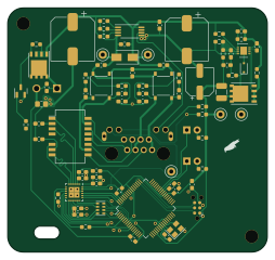
About the Gated Passthrough PCB
Gated Passthrough is an open source Silicon Labs PCB design by crawford, published on GitHub under the GPL-3.0 license. It is a 2-layer board measuring 63.5 × 59.7 mm, with 80 components from 49 distinct parts.
Its main chip is the EFM32GG11B8xx, from the Silicon Labs family. Other key parts include the KSZ8081RND, LM5085 and TPS2375-1. By type, the board carries 30 capacitors, 24 resistors, 6 diodes, 5 test points, 4 ICs and 4 inductors.
From the project
A base platform for PoE peripherals
This project makes use of git commit hooks. Configure git to use them by running the following from the root of the repository:
git config --local core.hooksPath .githooks/
Main components on the Gated Passthrough
Gated Passthrough bill of materials (BOM)
80 components, 49 distinct parts.
| Qty | Part | Footprint | Refs |
|---|---|---|---|
| 1 | EFM32GG11B8xx | QFP-64 | U1 |
| 1 | KSZ8081RND | QFN-24 | U2 |
| 1 | LM5085 | WSON-8-1EP_3x3mm_P0.5mm_EP1.6x2.0mm | U3 |
| 1 | TPS2375-1 | TSSOP-8_4.4x3mm_P0.65mm | U4 |
| 2 | Q_PMOS_DGS | PowerPAK_SO-8_Single | Q1, Q2 |
| 1 | Q_NPN_BEC | SOT-23 | Q3 |
| 1 | 50 MHz | Oscillator_SMD_Abracon_ASE-4Pin_3.2x2.5mm | X1 |
| 1 | RJ45_LED_Shielded | RJHSE-338X | J2 |
| 1 | Screw_Terminal_01x02 | Phoenix_1935161 | J3 |
| 1 | GND | TestPoint_Loop_D1.80mm_Drill1.0mm_Beaded | TP1 |
| 1 | VDD | TestPoint_Loop_D1.80mm_Drill1.0mm_Beaded | TP2 |
| 1 | VSS | TestPoint_Loop_D1.80mm_Drill1.0mm_Beaded | TP3 |
| 1 | EARTH | TestPoint_Loop_D1.80mm_Drill1.0mm_Beaded | TP4 |
| 1 | 3V3 | TestPoint_Loop_D1.80mm_Drill1.0mm_Beaded | TP5 |
| 1 | PT61017PEL | PT61017PEL | TR1 |
| 1 | ID | LED_D4.0mm | D1 |
| 1 | NET | LED_D4.0mm | D2 |
| 1 | D_Zener | D_SMA | D3 |
| 2 | D_Bridge_+-AA | Diode_Bridge_Diotec_ABS | D4, D6 |
| 1 | D_Schottky | D_SOD-323F | D5 |
Show 29 more
| Qty | Part | Footprint | Refs |
|---|---|---|---|
| 3 | Ferrite_Bead_Small | L_0603_1608Metric_Pad1.05x0.95mm_HandSolder | FB1, FB2, FB3 |
| 1 | 15u | L_1210_3225Metric_Pad1.42x2.65mm_HandSolder | L1 |
| 9 | 0u1 | C_0603_1608Metric_Pad1.08x0.95mm_HandSolder | C1, C2, C5, C6, C7, C10, C11, C18 +1 |
| 3 | 22u | C_0603_1608Metric_Pad1.08x0.95mm_HandSolder | C3, C4, C8 |
| 1 | 2u2 | C_0603_1608Metric_Pad1.08x0.95mm_HandSolder | C9 |
| 6 | 1n | C_0603_1608Metric_Pad1.08x0.95mm_HandSolder | C12, C16, C20, C23, C26, C30 |
| 1 | 33u | CP_Elec_10x10 | C13 |
| 4 | 10n | C_0603_1608Metric_Pad1.08x0.95mm_HandSolder | C14, C17, C19, C22 |
| 2 | 1u | C_0603_1608Metric_Pad1.08x0.95mm_HandSolder | C15, C29 |
| 1 | 0u47 | C_0603_1608Metric_Pad1.08x0.95mm_HandSolder | C21 |
| 1 | 47u | CP_Elec_10x12.5 | C24 |
| 1 | 3n3 | C_0603_1608Metric_Pad1.08x0.95mm_HandSolder | C27 |
| 1 | 100u | CP_Elec_6.3x5.8 | C28 |
| 2 | 1k | R_0603_1608Metric_Pad0.98x0.95mm_HandSolder | R1, R22 |
| 1 | 49R9 | R_0603_1608Metric_Pad0.98x0.95mm_HandSolder | R2 |
| 1 | 6k49 | R_0603_1608Metric_Pad0.98x0.95mm_HandSolder | R3 |
| 4 | 68R | R_0603_1608Metric_Pad0.98x0.95mm_HandSolder | R4, R5, R7, R8 |
| 4 | 75 | R_0603_1608Metric_Pad0.98x0.95mm_HandSolder | R6, R10, R12, R15 |
| 1 | 90k9 | R_0603_1608Metric_Pad0.98x0.95mm_HandSolder | R9 |
| 1 | 178k | R_0603_1608Metric_Pad0.98x0.95mm_HandSolder | R11 |
| 1 | 24k9 | R_0603_1608Metric_Pad0.98x0.95mm_HandSolder | R13 |
| 1 | 1k27 | R_0603_1608Metric_Pad0.98x0.95mm_HandSolder | R14 |
| 1 | 2k1 | R_0603_1608Metric_Pad0.98x0.95mm_HandSolder | R16 |
| 1 | 10m | R_0603_1608Metric_Pad0.98x0.95mm_HandSolder | R17 |
| 1 | 0R1 | R_0805_2012Metric_Pad1.20x1.40mm_HandSolder | R18 |
| 1 | 66k5 | R_0603_1608Metric_Pad0.98x0.95mm_HandSolder | R19 |
| 1 | 16k5 | R_0603_1608Metric_Pad0.98x0.95mm_HandSolder | R20 |
| 2 | 10k | R_0603_1608Metric_Pad0.98x0.95mm_HandSolder | R21, R23 |
| 1 | 49R9 | R_Cat16-4 | RN1 |
Gated Passthrough design files
The KiCad project lives in the crawford/PoE repository on GitHub; these links point at the commit this page was built from.
Gated Passthrough: common questions
What microcontroller does the Gated Passthrough use?
The Gated Passthrough is built around the EFM32GG11B8xx, from the Silicon Labs family.
How big is the Gated Passthrough PCB?
The Gated Passthrough measures 63.5 × 59.7 mm, has 2 copper layers and is 1.69 mm thick.
How many components are on the Gated Passthrough?
80 components, from 49 distinct parts. The full bill of materials is listed on this page.
Where can I download the Gated Passthrough design files?
From the crawford/PoE repository on GitHub, which has the KiCad layout and the schematic; the links under Design files point to each one.
Can I use the Gated Passthrough design in my own project?
Yes, under the terms of its GPL-3.0 license, which crawford chose for the repository.
Can I test firmware for the Gated Passthrough without the hardware?
Yes. HardLabs builds a simulation of the board from its netlist and BOM, so you can run and debug Silicon Labs firmware against it before you order a PCB.
More boards in PoE
Similar boards
 Silicon Labs
Tomu hardware
im-tomu
13 × 9.4 mm11 parts2LCC-BY-SA-4.0365 Silicon Labs
One key
ahtn
14.5 × 14.5 mm10 parts2LNo license96 Silicon Labs
2key
36.5 × 17.5 mm7 parts2LNo license96 Silicon Labs
Ble soil moisture sensor
Miceuz
170 × 18 mm33 parts2LApache-2.033 Silicon Labs
Ble soil moisture sensor pannel
170 × 36 mm29 parts2LApache-2.033 Silicon Labs
Ym2413 dev
andete
115 × 45 mm146 parts2LNo license25