
Hexa lang


About the Hexa lang PCB
Hexa lang is an open source FPGA PCB design by dancinlab, published on GitHub under the MIT license. It is a 4-layer board measuring 100 × 80 mm, with 10 components from 7 distinct parts.
Its main chip is the XC7A35T-1CSG324C, from the FPGA family. Other key parts include the TPS7A4901 → +5V (mixed), LTC2378-20, AD8429ARZ, ISO224ADWVR and TLP358. By type, the board carries 9 ICs and 1 connector.
It belongs with the usb & debug tools designs in this gallery.
From the project
💎 Native compiler with atlas-bound theorems — 8 strict-lint stages · citation-enforced · no LLVM · self-hosting native fixpoint
Per .roadmap.hexartsc §A.6.1 extension beyond Phase D+, this directory adds the schematic + EDA BOM + PCB stackup + Gerber-build script layer: the natural bridge from firmware/hdl/constraints.xdc (FPGA pin assignments) and firmware/mcu/chamberdrv.rs (MCU pinout) to actual PCB fabrication.
When KiCad is not installed, buildkicad.py exits cleanly with a SKIP message — Phase E1+ contract is "skeleton-checked-into-repo, verified-parse-when-toolchain-available". Output directory build/` is created on demand and gitignored.
Main components on the Hexa lang
Hexa lang bill of materials (BOM)
10 components, 7 distinct parts — part numbers from the project's BOM.
| Qty | Part | Footprint | Refs |
|---|---|---|---|
| 1 | XC7A35T-1CSG324C AMD/Xilinx | U1 | |
| 1 | TPS7A4901 → +5V (mixed) | U1B | |
| 2 | LTC2378-20 Analog Devices | U2, U3 | |
| 2 | AD8429ARZ AD8429 Analog Devices | U4, U5 | |
| 2 | ISO224ADWVR ISO224 Texas Instruments | U6, U7 | |
| 1 | TLP358 Toshiba | U8 | |
| 1 | 132289 +24V/2A DC jack Amphenol RF | J1 |
Hexa lang design files
The KiCad project lives in the dancinlab/hexa-lang repository on GitHub; these links point at the commit this page was built from.
Hexa lang: common questions
What microcontroller does the Hexa lang use?
The Hexa lang is built around the XC7A35T-1CSG324C, from the FPGA family.
How big is the Hexa lang PCB?
The Hexa lang measures 100 × 80 mm, has 4 copper layers and is 1.6 mm thick.
How many components are on the Hexa lang?
10 components, from 7 distinct parts, with part numbers taken from the project's own BOM. The full bill of materials is listed on this page.
Where can I download the Hexa lang design files?
From the dancinlab/hexa-lang repository on GitHub, which has the KiCad layout, the schematic and the BOM; the links under Design files point to each one.
Can I use the Hexa lang design in my own project?
Yes, under the terms of its MIT license, which dancinlab chose for the repository.
Can I test firmware for the Hexa lang without the hardware?
Yes. HardLabs builds a simulation of the board from its netlist and BOM, so you can run and debug FPGA firmware against it before you order a PCB.
Similar boards
 FPGA
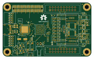
FPGABase board
GlasgowEmbedded
80 × 49 mm222 parts4L0BSD2.2k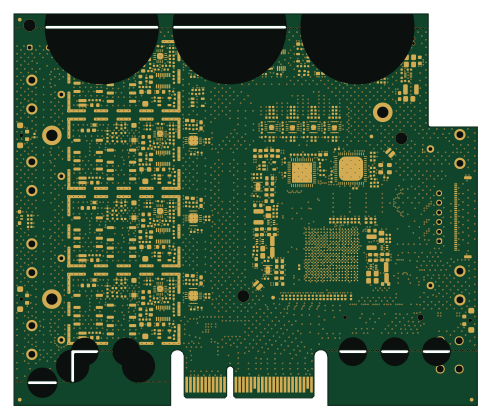 FPGA
FPGAThunderscope Rev5.3
EEVengers
122.5 × 103.5 mm817 parts6LMIT1.3k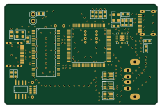 FPGA
FPGAUsb sniffer
ataradov
58.2 × 38.1 mm86 parts2LBSD-3-Clause1.3k FPGA
FPGATomu, I'm
theacodes
13 × 9.4 mm40 parts4LMIT1.1k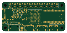 FPGA
FPGAIcepi zero
cheyao
65 × 30 mm143 parts4LSHL-2.1828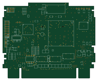 FPGA
FPGASd2snes
mrehkopf
101.5 × 83 mm147 partsGPL-2.0717