
DAC ADC PWM IO BACK UP

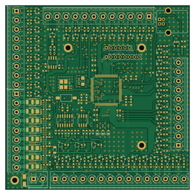
About the DAC ADC PWM IO BACK UP PCB
DAC ADC PWM IO BACK UP is an open source STM32 PCB design by DanielMartensson, published on GitHub under the MIT license. It is a 4-layer board measuring 100 × 100 mm, with 266 components from 41 distinct parts.
Its main chip is the STM32F373VBTx, from the STM32 family. Other key parts include the AP7343-33W5-7, LM2902, LM2904 and TCAN332. By type, the board carries 124 resistors, 44 diodes, 36 capacitors, 30 fuses, 11 transistors and 8 connectors.
From the project
STM32 microcontroller with lots of periferials such as ADC, differential ADC, Input Capture, PWM, USB, Encoder, DAC, Digital Input, RTC, CAN-bus + Alarm etc.
This project is a PCB bord that has the following measurement and control input/output:
12 x ADC at 16-bit resolution for 0-20mA input with programmable gain 5 x Differential ADC at 16-bit for 0-20mA input with programmable gain 3 x DAC at 12-bit with 0-20mA output 8 x PWM for 0-2.2A with N-channel MOSFET 10 x Digital Input 1 x CAN-bus channel 4 x Input Capture for 0 kHz to 10kHz 3 x Encoder for -32768 to 32767 pulses 1 x USB port for connecting with OpenSourceLogger and GoobySoft 1 x SPI with 3 chip select for ILI9341 LCD with touch 1 x ST-Link V2 connection 1 x RTC clock with two alarms…
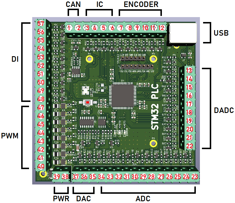
Main components on the DAC ADC PWM IO BACK UP
DAC ADC PWM IO BACK UP bill of materials (BOM)
266 components, 41 distinct parts.
| Qty | Part | Footprint | Refs |
|---|---|---|---|
| 1 | AP7343-33W5-7 | SOT-23-5 | U2 |
| 1 | LM2902 | SOIC-14_3.9x8.7mm_P1.27mm | U3 |
| 1 | STM32F373VBTx | LQFP-100_14x14mm_P0.5mm | U4 |
| 1 | LM2904 | SOIC-8_3.9x4.9mm_P1.27mm | U5 |
| 1 | TCAN332 | SOIC-8_3.9x4.9mm_P1.27mm | U6 |
| 3 | BC847C-QR | SOT-323_SC-70 | Q1, Q2, Q3 |
| 8 | BUK9M15-60EX | LFPAK33 | Q4, Q5, Q6, Q7, Q8, Q9, Q10, Q11 |
| 1 | HSE | Crystal_SMD_3225-4Pin_3.2x2.5mm_HandSoldering | Y1 |
| 1 | LSE | Crystal_SMD_EuroQuartz_EQ161-2Pin_3.2x1.5mm_HandSoldering | Y2 |
| 2 | Screw_Terminal_01x9 | TerminalBlock_Phoenix_PT-1,5-9-5.0-H_1x09_P5.00mm_Horizontal | J1, J16 |
| 1 | Screw_Terminal_01x02 | TerminalBlock_Phoenix_PT-1,5-2-5.0-H_1x02_P5.00mm_Horizontal | J2 |
| 1 | Conn_01x08 | PinHeader_1x08_P2.54mm_Vertical | J3 |
| 1 | Screw_Terminal_01x12 | TerminalBlock_Phoenix_PT-1,5-12-5.0-H_1x12_P5.00mm_Horizontal | J8 |
| 1 | USB_B | USB_B_OST_USB-B1HSxx_Horizontal | J9 |
| 1 | Screw_Terminal_01x15 | TerminalBlock_Phoenix_PT-1,5-15-5.0-H_1x15_P5.00mm_Horizontal | J14 |
| 1 | Screw_Terminal_01x10 | TerminalBlock_Phoenix_PT-1,5-10-5.0-H_1x10_P5.00mm_Horizontal | J15 |
| 1 | Battery_Cell | BatteryHolder_Keystone_3002_1x2032 | BT1 |
| 22 | Max 30mA | Fuse_0603_1608Metric | F1, F2, F3, F4, F5, F6, F7, F8 +14 |
| 8 | Max 2.5A | Fuse_1210_3225Metric | F13, F14, F15, F16, F17, F18, F19, F20 |
| 1 | ST-Link V2 connetor | PinHeader_1x06_P2.54mm_Vertical | STLINK2 |
Show 21 more
| Qty | Part | Footprint | Refs |
|---|---|---|---|
| 1 | SW_Push | SW_SPST_FSMSM | SW1 |
| 42 | BZX84C3V6LT1G | D_SOT-23_ANK | D1, D2, D3, D4, D5, D6, D7, D8 +34 |
| 1 | PESD5V0L2BT,215 | SOT-23 | D28 |
| 1 | SK56A-LTP | D_SMA | D44 |
| 1 | LED_USB_RX_TX | LED_0603_1608Metric | L0 |
| 1 | LED_CAN_RX_TX | LED_0603_1608Metric | L1 |
| 1 | LED_ERROR | LED_0603_1608Metric | L2 |
| 10 | 100nF | C_0603_1608Metric | C1, C6, C7, C11, C13, C21, C22, C24 +2 |
| 2 | 10pF | C_0402_1005Metric | C2, C3 |
| 7 | 1uF | C_0603_1608Metric | C4, C5, C9, C14, C18, C19, C27 |
| 3 | 4.7uF | C_0603_1608Metric | C8, C15, C30 |
| 11 | 10nF | C_0603_1608Metric | C10, C12, C16, C17, C25, C28, C33, C34 +3 |
| 2 | 4.7pF | C_0402_1005Metric | C20, C23 |
| 1 | 10uF | C_1206_3216Metric | C31 |
| 1 | 2k | R_0402_1005Metric | R1 |
| 82 | 10k | R_0603_1608Metric | R2, R7, R8, R9, R10, R11, R12, R13 +74 |
| 33 | 160 | R_0603_1608Metric | R3, R4, R5, R6, R14, R15, R16, R17 +25 |
| 1 | 1.5k | R_0603_1608Metric | R44 |
| 2 | 60 | R_0603_1608Metric | R53, R83 |
| 3 | 220 | R_0402_1005Metric | R54, R78, R79 |
| 2 | 0 | R_0402_1005Metric | R55, R56 |
DAC ADC PWM IO BACK UP design files
The KiCad project lives in the DanielMartensson/STM32-PLC repository on GitHub; these links point at the commit this page was built from.
DAC ADC PWM IO BACK UP: common questions
What microcontroller does the DAC ADC PWM IO BACK UP use?
The DAC ADC PWM IO BACK UP is built around the STM32F373VBTx, from the STM32 family.
How big is the DAC ADC PWM IO BACK UP PCB?
The DAC ADC PWM IO BACK UP measures 100 × 100 mm, has 4 copper layers and is 1.6 mm thick.
How many components are on the DAC ADC PWM IO BACK UP?
266 components, from 41 distinct parts. The full bill of materials is listed on this page.
Where can I download the DAC ADC PWM IO BACK UP design files?
From the DanielMartensson/STM32-PLC repository on GitHub, which has the KiCad layout; the links under Design files point to each one.
Can I use the DAC ADC PWM IO BACK UP design in my own project?
Yes, under the terms of its MIT license, which DanielMartensson chose for the repository.
Can I test firmware for the DAC ADC PWM IO BACK UP without the hardware?
Yes. HardLabs builds a simulation of the board from its netlist and BOM, so you can run and debug STM32 firmware against it before you order a PCB.
More boards in STM32-PLC
Similar boards
 STM32
STM32LumenPnP Motherboard
opulo-inc
149 × 95 mm296 parts4LCC-BY-SA-4.03.7k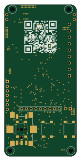 STM32
STM32AxxSolder
AxxAxx
39 × 82.5 mm122 parts2LGPL-3.01.7k STM32
STM32AIOC
skuep
21 × 31.5 mm47 parts2LMIT1.4k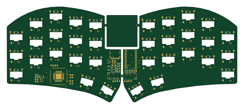 STM32
STM32Ferris
pierrechevalier83
208.8 × 86.8 mm102 parts2LSHL-2.11.3k STM32
STM32176 pin board
rusefi
61.8 × 73.2 mm76 parts2LGPL-3.01.2k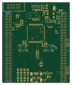 STM32
STM32Brain board STM32F407
61.8 × 73.2 mm69 parts2LGPL-3.01.2k