
Attiny85 NFC MULTI TAG

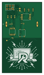
About the Attiny85 NFC MULTI TAG PCB
Attiny85 NFC MULTI TAG is an open source AVR/Arduino PCB design by dgm91-pro, published on GitHub. It is a 2-layer board measuring 35 × 62 mm, with 15 components from 12 distinct parts.
Its main chip is the ATtiny85V-10S, from the AVR/Arduino family. Other key parts include the ST25DV04KC-IE6S3 and APTF1616LSEEZGKQBKC. By type, the board carries 6 resistors, 3 ICs, 3 capacitors, 1 switch and 1 inductor.
It belongs with the power & battery designs in this gallery.
From the project
A small Project in bond with hackclub YSWS
See HACKCLUBREQUEST.md` for the message prepared for Hack Club.
A compact, battery-powered NFC keychain built around an ATtiny85V and an ST25DV04KC dynamic NFC tag. A single button switches between four configurable URL profiles, each indicated by an RGB LED.
- Four selectable NFC URL profiles: blue, red, green, and violet - One-button interface - RGB LED feedback - NFC is disabled when the device starts and when it is switched off - Selected profile is saved in the ATtiny85 EEPROM - Low-power sleep while switched off - I²C error feedback: four yellow flashes
Main components on the Attiny85 NFC MULTI TAG
Attiny85 NFC MULTI TAG bill of materials (BOM)
15 components, 12 distinct parts.
| Qty | Part | Footprint | Refs |
|---|---|---|---|
| 1 | ATtiny85V-10S | SOIC-8_5.3x5.3mm_P1.27mm | U1 |
| 1 | ST25DV04KC-IE6S3 | SO-8_STM | U2 |
| 1 | APTF1616LSEEZGKQBKC | SON4_APTF1616LSEEZGKQBKC_KNB_fixed | U3 |
| 1 | BC2032-E2 | BC2032-E2_MPD | B1 |
| 1 | PTS526 SM15 SMTR2 LFS | SON4_PTS526 SM15 SMTR2 LFS_CNK | SW1 |
| 1 | L | ANT_Spiral_v3 | L1 |
| 1 | CL21B106KOQNNNE | CAP_CL21B106KOQNNNE_SAM | C1 |
| 2 | CL10B104KO8NNNC | CAP_CL10_SAM | C2, C3 |
| 1 | RMCF0603FT470R | STA_RMCF0603_STP | R1 |
| 1 | RMCF0603FT220R | STA_RMCF0603_STP | R2 |
| 1 | RMCF0603FT33R0 | STA_RMCF0603_STP | R3 |
| 3 | RMCF0603FT10K0 | STA_RMCF0603_STP | R4, R5, R6 |
Attiny85 NFC MULTI TAG design files
The KiCad project lives in the dgm91-pro/Attiny85_NFC_MULTI_TAG repository on GitHub; these links point at the commit this page was built from.
- LayoutKiCad/tag.kicad_pcb
- SchematicKiCad/tag.kicad_sch
Attiny85 NFC MULTI TAG: common questions
What microcontroller does the Attiny85 NFC MULTI TAG use?
The Attiny85 NFC MULTI TAG is built around the ATtiny85V-10S, from the AVR/Arduino family.
How big is the Attiny85 NFC MULTI TAG PCB?
The Attiny85 NFC MULTI TAG measures 35 × 62 mm, has 2 copper layers and is 1.6 mm thick.
How many components are on the Attiny85 NFC MULTI TAG?
15 components, from 12 distinct parts. The full bill of materials is listed on this page.
Where can I download the Attiny85 NFC MULTI TAG design files?
From the dgm91-pro/Attiny85_NFC_MULTI_TAG repository on GitHub, which has the KiCad layout and the schematic; the links under Design files point to each one.
Can I use the Attiny85 NFC MULTI TAG design in my own project?
The repository has no license, so all rights stay with dgm91-pro. Use it as a reference, and ask the author before reusing the design.
Can I test firmware for the Attiny85 NFC MULTI TAG without the hardware?
Yes. HardLabs builds a simulation of the board from its netlist and BOM, so you can run and debug AVR/Arduino firmware against it before you order a PCB.
Similar boards
 AVR/Arduino
Magspoof
samyk
35 × 29 mm11 parts2LNo license4.2k AVR/Arduino
Redox keyboard
mattdibi
162.2 × 126.5 mm77 parts2LMIT2.0k AVR/Arduino
Labrador
espotek-org
36.8 × 34.7 mm75 parts2LNo license1.2k AVR/Arduino
V4
stuartpittaway
30 × 50 mm38 parts2LCC-BY-NC-4.01.1k AVR/Arduino
ModuleV450
30 × 61.4 mm39 parts2LCC-BY-NC-4.01.1k AVR/Arduino
Discipline
coseyfannitutti
304.9 × 122.8 mm170 parts2LCC-BY-NC-4.01.0k