
ZRAD Z-Wave Reference Application Design

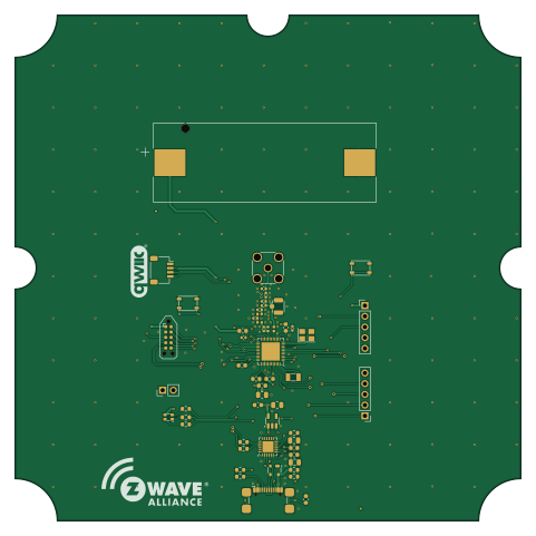
About the ZRAD Z-Wave Reference Application Design PCB
ZRAD Z-Wave Reference Application Design is an open source Silicon Labs PCB design by drzwave, published on GitHub under the MIT license. It is a 4-layer board measuring 120 × 120 mm, with 55 components from 38 distinct parts.
Its main chip is the EFR32xG23xxxxF512xM48, from the Silicon Labs family. Other key parts include the AP2127K-3.3 and CP2102N-Axx-xQFN24. By type, the board carries 19 capacitors, 10 resistors, 8 connectors, 8 inductors, 3 ICs and 2 crystals.
From the project
Z-Wave USB Controller with best-in-class RF range Reference Design
Z-Wave USB Controller with best-in-class RF range Reference Application Design
The Z-Wave Alliance Z-Wave Reference Application Design (ZRAD) is a simple to copy, easy to modify, Open-Source Reference design of a Z-Wave best-in-class RF range device. ZRAD is not a product you can purchase, but anyone is welcome to manufacture and sell a product based on ZRAD. The objective is to accelerate Time-To-Market for Z-Wave products thru a simple to follow example with detailed step-by-step instructions. See the docs/ZRADTechDocs.docx file for more details and the Theory of Operation.
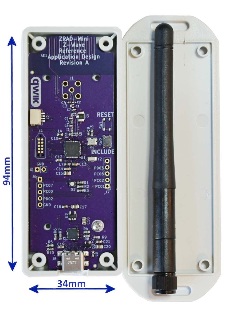
Main components on the ZRAD Z-Wave Reference Application Design
ZRAD Z-Wave Reference Application Design bill of materials (BOM)
55 components, 38 distinct parts.
| Qty | Part | Footprint | Refs |
|---|---|---|---|
| 1 | EFR32xG23xxxxF512xM48 | QFN-48-1EP_6x6mm_P0.4mm_EP4.3x4.3mm | U1 |
| 1 | AP2127K-3.3 | SOT-23-5 | U2 |
| 1 | CP2102N-Axx-xQFN24 | QFN-24-1EP_4x4mm_P0.5mm_EP2.6x2.6mm | U3 |
| 1 | 32768Hz | Crystal_SMD_3215-2Pin_3.2x1.5mm | Y1 |
| 1 | 39MHz 10ppm | Crystal_SMD_3225-4Pin_3.2x2.5mm | Y2 |
| 1 | Qwiic_RA | JST_SH_SM04B-SRSS-TB_1x04-1MP_P1.00mm_Horizontal | J1 |
| 1 | Conn_Coaxial | SMA_Wurth_60312002114503_Vertical | J2 |
| 1 | Conn_02x05_Odd_Even | Tag-Connect_TC2050-IDC-NL_2x05_P1.27mm_Vertical | J3 |
| 1 | Conn_Coaxial | U.FL_Hirose_U.FL-R-SMT-1_Vertical | J4 |
| 2 | Conn_01x05 | PinHeader_1x05_P2.54mm_Vertical | J5, J7 |
| 1 | Conn_01x02 | PinHeader_1x02_P2.54mm_Vertical | J6 |
| 1 | USB_C_Receptacle_USB2.0_16P | USB_C_Receptacle_GCT_USB4110 | J8 |
| 1 | CR123 | 1050_KEY | BT1 |
| 2 | PTS810 | SW_SPST_PTS810 | SW1, SW2 |
| 1 | QLSP14RGB_B | LED_QLSP14RGB | D1 |
| 1 | SP0503BAHT | SOT-143 | D2 |
| 3 | 33@100 | L_0603_1608Metric | L1, L5, L8 |
| 1 | 1N3 | L_0402_1005Metric | L2 |
| 1 | 13N | L_0402_1005Metric | L3 |
| 1 | 1N5 | L_0402_1005Metric | L4 |
Show 18 more
| Qty | Part | Footprint | Refs |
|---|---|---|---|
| 1 | 18N | L_0402_1005Metric | L6 |
| 1 | 2U2 | L_0603_1608Metric | L7 |
| 2 | NM | C_0402_1005Metric | C1, C10 |
| 3 | 220P | C_0402_1005Metric | C2, C3, C7 |
| 1 | 47P | C_0402_1005Metric | C4 |
| 1 | 1P3 | C_0402_1005Metric | C5 |
| 3 | 1UF | C_0603_1608Metric | C6, C15, C18 |
| 1 | 7P2 | C_0402_1005Metric | C8 |
| 1 | 1P9 | C_0402_1005Metric | C9 |
| 3 | 100N | C_0603_1608Metric | C11, C16, C19 |
| 4 | 4U7 | C_0805_2012Metric | C12, C13, C14, C17 |
| 1 | 820 | R_0603_1608Metric | R1 |
| 1 | 1K2 | R_0603_1608Metric | R2 |
| 2 | 1K | R_0603_1608Metric | R3, R9 |
| 2 | 100 | R_0603_1608Metric | R4, R5 |
| 1 | 47K5 | R_0603_1608Metric | R6 |
| 1 | 22K1 | R_0603_1608Metric | R7 |
| 2 | 5K1 | R_0603_1608Metric | R8, R10 |
ZRAD Z-Wave Reference Application Design design files
The KiCad project lives in the drzwave/ZRAD repository on GitHub; these links point at the commit this page was built from.
- Layouthardware/ZRAD/ZRAD.kicad_pcb
- Schematichardware/ZRAD/ZRAD.kicad_sch
ZRAD Z-Wave Reference Application Design: common questions
What microcontroller does the ZRAD Z-Wave Reference Application Design use?
The ZRAD Z-Wave Reference Application Design is built around the EFR32xG23xxxxF512xM48, from the Silicon Labs family.
How big is the ZRAD Z-Wave Reference Application Design PCB?
The ZRAD Z-Wave Reference Application Design measures 120 × 120 mm, has 4 copper layers and is 1.6 mm thick.
How many components are on the ZRAD Z-Wave Reference Application Design?
55 components, from 38 distinct parts. The full bill of materials is listed on this page.
Where can I download the ZRAD Z-Wave Reference Application Design design files?
From the drzwave/ZRAD repository on GitHub, which has the KiCad layout and the schematic; the links under Design files point to each one.
Can I use the ZRAD Z-Wave Reference Application Design design in my own project?
Yes, under the terms of its MIT license, which drzwave chose for the repository.
Can I test firmware for the ZRAD Z-Wave Reference Application Design without the hardware?
Yes. HardLabs builds a simulation of the board from its netlist and BOM, so you can run and debug Silicon Labs firmware against it before you order a PCB.
More boards in ZRAD
Similar boards
 Silicon Labs
Tomu hardware
im-tomu
13 × 9.4 mm11 parts2LCC-BY-SA-4.0365 Silicon Labs
Ble soil moisture sensor
Miceuz
170 × 18 mm33 parts2LApache-2.033 Silicon Labs
Ble soil moisture sensor pannel
170 × 36 mm29 parts2LApache-2.033 Silicon Labs
MWGEN-G1
MR-DOS
100 × 100 mm341 parts4LGPL-3.018 Silicon Labs
Efm32wg
dragonlock2
32 × 32 mm61 parts2LApache-2.013 Silicon Labs
DSMR-Splitter
basilfx
59.9 × 39.9 mm53 parts2LCC-BY-NC-4.07