
Splitflap Display

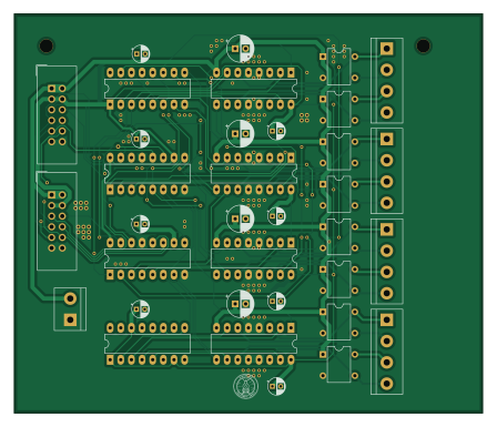
About the Splitflap Display PCB
Splitflap Display is an open source PCB design by dylanmsu, published on GitHub under the GPL-3.0 license. It is a 2-layer board measuring 111.8 × 95.3 mm, with 35 components from 9 distinct parts.
Other key parts include the CD4049UBE, 74HC595 and SN754410NE. By type, the board carries 12 capacitors, 8 ICs, 8 diodes and 5 connectors.
It belongs with the displays & leds designs in this gallery.
From the project
software to drive a public split flap display
That line of code will flip the segment once. Or if you want more control, there is the method:
It sets the state of the selected h-Bridge. There are (in the future) a bunch of example sketches with different use cases for the library. However, they all require at least one driver PCB to actually drive the split flap modules.
V1: first version, fully made in kicad with through hole components V4: latest version, made in EasyEDA with mostly SMD components
Main components on the Splitflap Display
Splitflap Display bill of materials (BOM)
35 components, 9 distinct parts — part numbers from the project's BOM.
| Qty | Part | Footprint | Refs |
|---|---|---|---|
| 2 | CD4049UBE | DIP-16_W7.62mm_LongPads | IC1, IC2 |
| 2 | 74HC595 | DIP-16_W7.62mm_LongPads | U1, U2 |
| 4 | SN754410NE | DIP-16_W7.62mm_LongPads | U3, U4, U5, U6 |
| 4 | Screw_Terminal_01x04 | TerminalBlock_bornier-4_P5.08mm | J3, J4, J5, J6 |
| 1 | Screw_Terminal_01x02 | TerminalBlock_bornier-2_P5.08mm | J7 |
| 2 | Conn_02x06_Odd_Even | IDC-Header_2x06_P2.54mm_Vertical | INPUT J1, OUTPUT J2 |
| 8 | D_Bridge_+-AA | Diode_Bridge_DIP-4_W7.62mm_P5.08mm | D1, D2, D3, D4, D5, D6, D7, D8 |
| 8 | CP | CP_Radial_D4.0mm_P2.00mm | C1, C2, C3, C4, C6, C7, C9, C10 |
| 4 | CP | CP_Radial_D6.3mm_P2.50mm | C5, C8, C11, C12 |
Splitflap Display design files
The KiCad project lives in the dylanmsu/Splitflap_Display repository on GitHub; these links point at the commit this page was built from.
Splitflap Display: common questions
How big is the Splitflap Display PCB?
The Splitflap Display measures 111.8 × 95.3 mm, has 2 copper layers and is 1.6 mm thick.
How many components are on the Splitflap Display?
35 components, from 9 distinct parts, with part numbers taken from the project's own BOM. The full bill of materials is listed on this page.
Where can I download the Splitflap Display design files?
From the dylanmsu/Splitflap_Display repository on GitHub, which has the KiCad layout and the BOM; the links under Design files point to each one.
Can I use the Splitflap Display design in my own project?
Yes, under the terms of its GPL-3.0 license, which dylanmsu chose for the repository.
Similar boards

LevelShifterBreakout
scottbez1
15.2 × 20.3 mm5 parts2LApache-2.022.2k
View base
81.2 × 81.2 mm81 parts2LApache-2.022.2k
View screen
35 × 35 mm12 parts2LApache-2.022.2k
BM28B0.6-24DSBreakout
15.2 × 35.6 mm3 parts2LApache-2.022.2k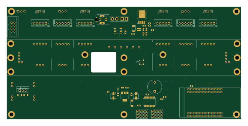
ChainlinkDriverTester
198.1 × 95.3 mm123 parts2LApache-2.04.2k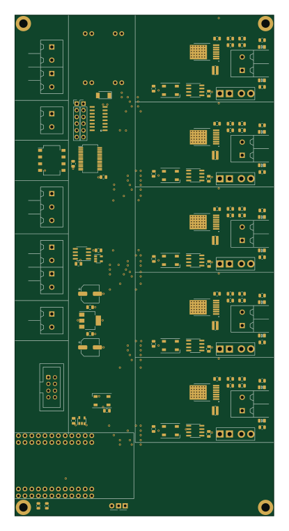
ChainlinkBase
98.4 × 190.5 mm119 parts2LApache-2.04.2k