
Complete input routed

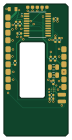
About the Complete input routed PCB
Complete input routed is an open source PCB design by earlynerd, published on GitHub. It is a 4-layer board measuring 17 × 35 mm, with 23 components from 19 distinct parts.
Other key parts include the DRV2625YFFR and M2003FC1AE. By type, the board carries 7 capacitors, 7 resistors, 5 connectors, 2 ICs, 1 module and 1 fuse.
From the project
Open main/main.kicadpro and satellite/satellite.kicadpro in KiCad 10.
Open main/main.kicadpro and satellite/satellite.kicadpro in KiCad 10.
- main/: one controller daughterboard PCBA; its haptic pod is a separate universal board. - satellite/: one universal PCBA, built eight times per wrist. JP1 selects normal or end-of-chain operation. - HapticBracelet.kicadsym, HapticBracelet.pretty/: shared libraries referenced by both projects. - panel/: future derived manufacturing panel, never the source for board edits. - verification/project-split/: current schematic PDFs, previews and check reports. - archive/combined-project/: superseded eight-island project…
Main components on the Complete input routed
Complete input routed bill of materials (BOM)
23 components, 19 distinct parts.
| Qty | Part | Footprint | Refs |
|---|---|---|---|
| 1 | DRV2625YFFR DRV2625 Texas Instruments | DRV2625_YFF_9_0.4mm | U9 |
| 1 | M2003FC1AE Nuvoton | TSSOP-20_4.4x6.5mm_P0.65mm | U24 |
| 1 | VLV041235L Vybronics | Vybronics_VLV041235L_FPC_Contact_Draft | M7 |
| 1 | CHAIN IN | WirePads_6_P2mm | J124 |
| 1 | CHAIN OUT | WirePads_6_P2mm | J125 |
| 1 | ICE / INITIAL FLASH | WirePads_5_P1.27mm | J126 |
| 1 | NTC (optional) | WirePads_2_P2mm | J127 |
| 1 | PROTECTED CELL 90mAh | WirePads_2_P2mm | J206 |
| 1 | 0467.250NR 250mA FAST Littelfuse | Fuse_Littelfuse_467_0603 | F106 |
| 3 | 100n | C_0402_1005Metric | C23, C24, C160 |
| 1 | 1u | C_0402_1005Metric | C25 |
| 1 | 10u | C_0805_2012Metric | C161 |
| 1 | 10n | C_0402_1005Metric | C162 |
| 1 | 22u 10V X5R | C_0805_2012Metric | C163 |
| 2 | 4.7k | R_0402_1005Metric | R20, R21 |
| 1 | 0 | R_0402_1005Metric | R160 |
| 1 | 33 | R_0402_1005Metric | R161 |
| 2 | 100k | R_0402_1005Metric | R162, R163 |
| 1 | 10k 1% | R_0402_1005Metric | R165 |
Complete input routed design files
The KiCad project lives in the earlynerd/ELRS-haptics repository on GitHub; these links point at the commit this page was built from.
Complete input routed: common questions
How big is the Complete input routed PCB?
The Complete input routed measures 17 × 35 mm, has 4 copper layers and is 0.8 mm thick.
How many components are on the Complete input routed?
23 components, from 19 distinct parts. The full bill of materials is listed on this page.
Where can I download the Complete input routed design files?
From the earlynerd/ELRS-haptics repository on GitHub, which has the KiCad layout; the links under Design files point to each one.
Can I use the Complete input routed design in my own project?
The repository has no license, so all rights stay with earlynerd. Use it as a reference, and ask the author before reusing the design.
More boards in ELRS-haptics
 ESP32
ESP32Merged
21 × 55.9 mm261 parts4LNo license0 ESP32
ESP32Candidate
21 × 55.9 mm261 parts4LNo license0 ESP32
ESP32Input
21 × 55.9 mm69 parts4LNo license0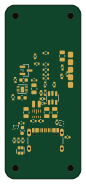 ESP32
ESP32Main
20 × 46 mm47 parts4LNo license0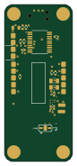
Haptic bracelet / satellite PCBA
20 × 46 mm26 parts4LNo license0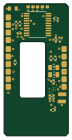
Pod-7-routed
17 × 35 mm24 parts4LNo license0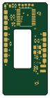
Pod-7
17 × 35 mm24 parts4LNo license0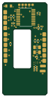
Completed template
17 × 35 mm23 parts4LNo license0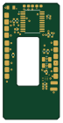
Pod-6
17 × 35 mm23 parts4LNo license0