
Cicada 4G

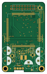
About the Cicada 4G PCB
Cicada 4G is an open source PCB design by EnAccess, published on GitHub under the MIT license. It is a 4-layer board measuring 40 × 65 mm, with 85 components from 34 distinct parts.
Other key parts include the SIM7600CE-L1C, USBLC6-2SC6 and M3406-ADJ. By type, the board carries 27 resistors, 24 capacitors, 11 diodes, 8 transistors, 8 connectors and 4 inductors.
It belongs with the iot & wireless designs in this gallery.
From the project
IoT Communications Module for Energy Access. A quick way to get production ready, bi-directional communications for your IoT embedded device.
This repository contains the hardware design of IOT embedded bi-directional communications device. through 2G, 3G, 4G modemsTech.
Checkout the examples in the firmware repository here
If you are only interested in manufacturing the PCBs, you only need files in the /manufacturing/ directory. send them to your contract manufacturer of choice,Some examples of other turnkey PCBA manufacturers are:
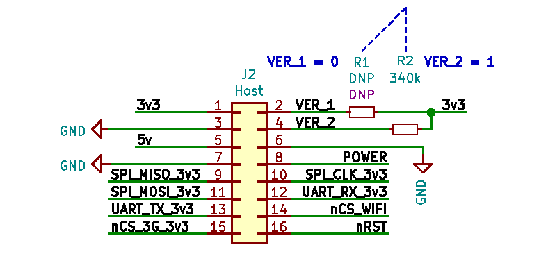
Main components on the Cicada 4G
Cicada 4G bill of materials (BOM)
85 components, 34 distinct parts — part numbers from the project's BOM.
| Qty | Part | Footprint | Refs |
|---|---|---|---|
| 1 | SIM7600CE-L1C sim7600 Simcom | sim7600 | U1 |
| 1 | USBLC6-2SC6 STM | SOT-23-6 | U2 |
| 1 | M3406-ADJ XI'AN Aerosemi Tech | TSOT-23-5 | U3 |
| 7 | WST3400S NMOS Winsok Semicon | SOT-23 | Q1, Q2, Q4, Q5, Q6, Q7, Q8 |
| 1 | AO3401 PMOS Guangdong Hottech | SOT-23 | Q3 |
| 1 | C30867 Host Boom Precision Elec | PinSocket_2x08_P2.54mm_Vertical_padded | J2 |
| 1 | C10418 USB_OTG Jing Extension of the Electronic | ZX62D-B-5PA8 | J3 |
| 4 | U.FL-R-SMT-1(80) IPX Hirose | U.FL_Molex_MCRF_73412-0110_Vertical | J4, J5, J6, J8 |
| 1 | Conn_01x04 | JST_PH_S4B-PH-SM4-TB_1x04-1MP_P2.00mm_Horizontal | J7 |
| 1 | SK-C793 Shenzhen Shengkai Electronics | SK-C793 | P1 |
| 6 | ESD5Z3V3 TVS Tak Cheong | D_SOD-523 | D1, D2, D3, D5, D8, D9 |
| 1 | BL-HB336G-TRB LED_B BrtLed | D_0603_1608Metric | D4 |
| 2 | LXES15AAA1-153 TVS Murata | D_0402_1005Metric | D6, D7 |
| 2 | SS14F SS14 MDD | D_SMA | D10, D11 |
| 1 | SDCL1005C47NJTDF 47nH Sunlord | L_0402_1005Metric | L1 |
| 2 | DNP | L_0402_1005Metric | L2, L3 |
| 1 | FPI0403F-3R3M 3.3uH 2A TAITEC | L_4030_Handsoldering | L4 |
| 5 | CL10B104KB8NNNC 0.1uF 50v X5R SAMSUNG | C_0603_1608Metric | C1, C8, C17, C18, C21 |
| 4 | CL05C330JB5NNNC 33pF C0G SAMSUNG | C_0402_1005Metric | C2, C3, C4, C13 |
| 5 | C3299 1000uF 10v CX | CP_Radial_D8.0mm_P3.50mm | C5, C14, C15, C23, C24 |
Show 14 more
| Qty | Part | Footprint | Refs |
|---|---|---|---|
| 5 | DNP | C_0402_1005Metric | C6, C9, C10, C11, C12 |
| 2 | CL10A105KB8NNNC 1uF 16v X5R SAMSUNG | C_0603_1608Metric | C7, C16 |
| 2 | CL21A226MOQNNNE 22uF 16v X5R SAMSUNG | C_0805_2012Metric | C19, C22 |
| 1 | CL05C101JB5NNNC 100pF C0G SAMSUNG | C_0402_1005Metric | C20 |
| 1 | 0402WGF5492TCE 54.9k UNI-ROYAL | R_0402_1005Metric | R1 |
| 1 | 0402WGF3403TCE 340k UNI-ROYAL | R_0402_1005Metric | R2 |
| 12 | 0402WGF4701TCE 4.7k UNI-ROYAL | R_0402_1005Metric | R3, R4, R5, R6, R17, R18, R20, R21 +4 |
| 3 | 0402WGF220JTCE 22R UNI-ROYAL | R_0402_1005Metric | R7, R8, R9 |
| 1 | 0402WGF4700TCE 470R UNI-ROYAL | R_0402_1005Metric | R10 |
| 2 | 0402WGF4022TCE 40.2k UNI-ROYAL | R_0402_1005Metric | R11, R22 |
| 4 | 0402WGF0000TCE 0R UNI-ROYAL | R_0402_1005Metric | R12, R13, R14, R15 |
| 1 | 0402WGF100JTCE 10R UNI-ROYAL | R_0402_1005Metric | R16 |
| 1 | 40.2k | R_0402_1005Metric | R19 |
| 1 | 6.98k | R_0402_1005Metric | R23 |
Cicada 4G design files
The KiCad project lives in the EnAccess/Cicada-GSM-HW repository on GitHub; these links point at the commit this page was built from.
Cicada 4G: common questions
How big is the Cicada 4G PCB?
The Cicada 4G measures 40 × 65 mm, has 4 copper layers and is 1.6 mm thick.
How many components are on the Cicada 4G?
85 components, from 34 distinct parts, with part numbers taken from the project's own BOM. The full bill of materials is listed on this page.
Where can I download the Cicada 4G design files?
From the EnAccess/Cicada-GSM-HW repository on GitHub, which has the KiCad layout, the schematic and the BOM; the links under Design files point to each one.
Can I use the Cicada 4G design in my own project?
Yes, under the terms of its MIT license, which EnAccess chose for the repository.
More boards in Cicada-GSM-HW
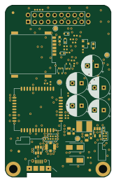
Similar boards

RPi RM0 WiFi/Bluetooth Module
schlae
11.1 × 14 mm76 parts6LNo license1.0k
L0 IMU MPU9250
Luos-io
20.3 × 15.2 mm7 parts2LMIT547
L0 USBA
20.3 × 15.3 mm19 parts2LMIT547
L0 Controller motor
20.3 × 15.3 mm11 parts2LMIT547
L0 Dynamixel
20.3 × 15.2 mm15 parts2LMIT547
L0 stepper driver
20.3 × 15.2 mm18 parts2LMIT547