
Panel

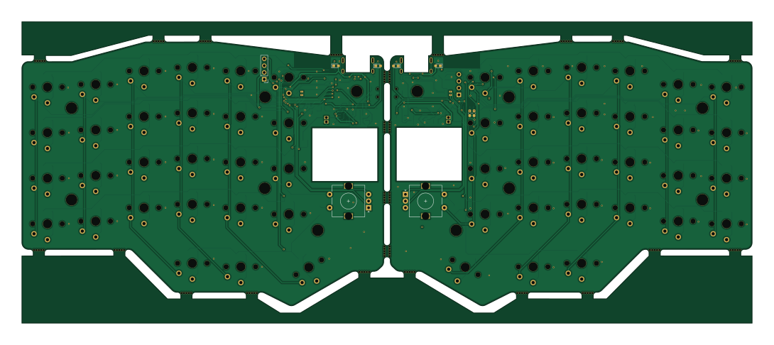
About the Panel PCB
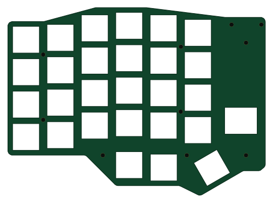
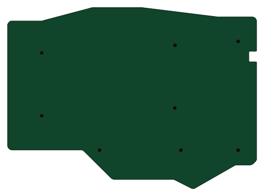
Panel is an open source PCB design by ericrlau, published on GitHub under the CC-BY-SA-4.0 license. It is a 2-layer board measuring 272.1 × 112.3 mm, with 80 components from 23 distinct parts.
Other key parts include the LN2054Y42AMR, E73-2G4M08S1C and AP2112K-3.3. By type, the board carries 31 diodes, 28 switches, 8 resistors, 5 capacitors, 3 ICs and 2 connectors.
It belongs with the keyboards and iot & wireless designs in this gallery.
From the project
Bluetooth low engery keyboard. Layout based on Sofle keyboard with some modifications. NRF52840 powered. Designed around Kaihl Choc switches and spacing.
- See ZMK docs for instructions on setting up ZMK and custimizing firmware. https://zmkfirmware.dev/docs/user-setup/ https://zmkfirmware.dev/docs/customization - Default *.uf2 files are pre-loaded on assembled pcbs. If you sourced and assembled your own pcb, you can file deafult pre-built firmware here: - https://github.com/ericrlau/COBO-zmk-config/releases
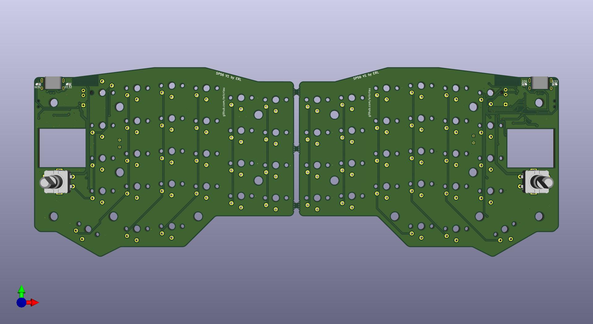
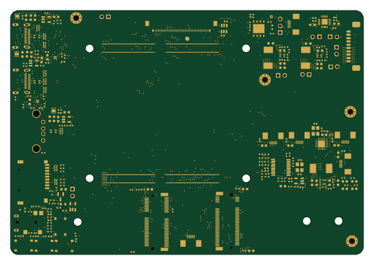
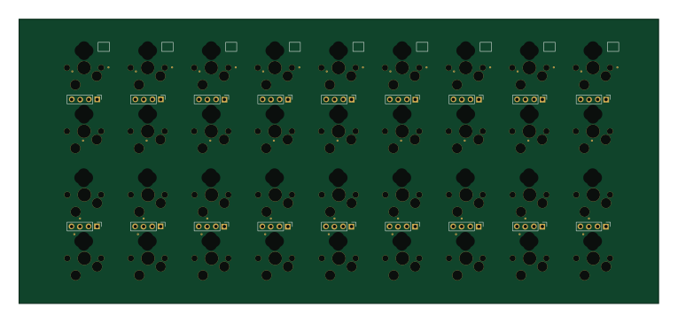
Main components on the Panel
Panel bill of materials (BOM)
80 components, 23 distinct parts.
| Qty | Part | Footprint | Refs |
|---|---|---|---|
| 1 | LN2054Y42AMR | SOT-23-5 | U1 |
| 1 | E73-2G4M08S1C | E73-2G4M08S1C-52840_minimal_inside_pads | U2 |
| 1 | AP2112K-3.3 | SOT-23-5 | U3 |
| 1 | A03407 | SOT-23 | Q2 |
| 1 | 32.768kHz | Crystal_SMD_MicroCrystal_CM9V-T1A-2Pin_1.6x1.0mm_HandSoldering | Y1 |
| 1 | USB_C_Receptacle_USB2.0 | USB-C_C168688 | J1 |
| 1 | SM02B-SRSS-TB(LF)(SN) | SM02B-SRSS-TB(LF)(SN) | J12 |
| 26 | SW_PUSH | KailhLowProfile | SW1, SW2, SW3, SW4, SW5, SW6, SW7, SW8 +18 |
| 1 | Rotary_Encoder_Switch | RotaryEncoder_Alps_EC11E-Switch_Vertical_H20mm | SW25 |
| 1 | SW_PUSH | KailhLowProfile_1.5U | SW26 |
| 1 | Conn_01x04_Female | PinHeader_1x04_P2.54mm_Vertical | SWD/C1 |
| 28 | D | D_SOD-123 | D1, D2, D3, D4, D5, D6, D7, D8 +20 |
| 2 | LED | LED_0603_1608Metric_Pad1.05x0.95mm_HandSolder | D31, D32 |
| 1 | 1N5819 | D_SOD-323_HandSoldering | D33 |
| 2 | 4.7uF | C_0603_1608Metric_Pad1.08x0.95mm_HandSolder | C1, C2 |
| 2 | 22pF | C_0603_1608Metric_Pad1.08x0.95mm_HandSolder | C3, C4 |
| 1 | 10uF | C_0603_1608Metric_Pad1.08x0.95mm_HandSolder | C5 |
| 2 | 1k | R_0603_1608Metric_Pad0.98x0.95mm_HandSolder | R1, R6 |
| 1 | 10k | R_0603_1608Metric_Pad0.98x0.95mm_HandSolder | R2 |
| 1 | 820k | R_0603_1608Metric_Pad0.98x0.95mm_HandSolder | R4 |
Show 3 more
| Qty | Part | Footprint | Refs |
|---|---|---|---|
| 1 | 2M | R_0603_1608Metric_Pad0.98x0.95mm_HandSolder | R5 |
| 2 | 5.1k | R_0603_1608Metric_Pad0.98x0.95mm_HandSolder | R7, R8 |
| 1 | 100k | R_0603_1608Metric_Pad0.98x0.95mm_HandSolder | R9 |
Panel design files
The KiCad project lives in the ericrlau/SP56 repository on GitHub; these links point at the commit this page was built from.
Panel: common questions
How big is the Panel PCB?
The Panel measures 272.1 × 112.3 mm, has 2 copper layers and is 1.6 mm thick.
How many components are on the Panel?
80 components, from 23 distinct parts. The full bill of materials is listed on this page.
Where can I download the Panel design files?
From the ericrlau/SP56 repository on GitHub, which has the KiCad layout; the links under Design files point to each one.
Can I use the Panel design in my own project?
Yes, under the terms of its CC-BY-SA-4.0 license, which ericrlau chose for the repository.
 byrantech


 google