
Lens

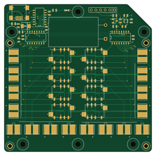
About the Lens PCB
Lens is an open source PIC PCB design by ervanalb, published on GitHub. It is a 4-layer board measuring 80 × 80 mm, with 53 components from 23 distinct parts.
Its main chip is the PIC16F1454, from the PIC family. Other key parts include the G6K-2F-RF, 3v3, 74LS595 and MMA8653FC. By type, the board carries 22 connectors, 13 ICs, 9 capacitors, 6 resistors, 2 diodes and 1 inductor.
From the project
Tap live cabling for inspection and injection
lens is a framework that allows you to tap live cabling for inspection and injection.
Watch the video of our presentation here!
Slides & whitepaper are available in the docs/ folder.
Or, photos of the device we presented can be found here.
You can reach us through github, or our emails are listed in our github profiles (Zach, Eric).
The wires of a network cable can be punched down into the lens tap board in two places without interrupting the packet flow. The tap board then provides a redundant copper path through a set of relays. Once all of the wires have been punched down on both…
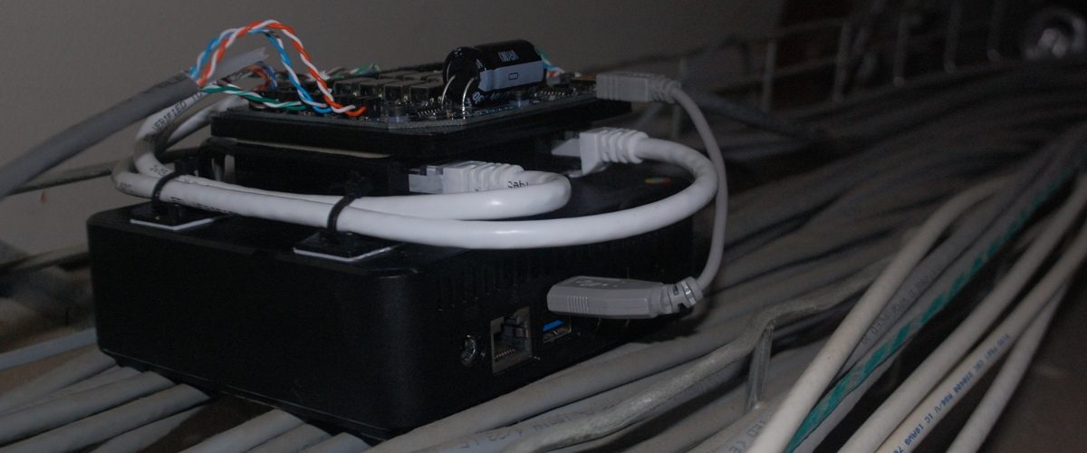
Main components on the Lens
Lens bill of materials (BOM)
53 components, 23 distinct parts.
| Qty | Part | Footprint | Refs |
|---|---|---|---|
| 8 | G6K-2F-RF | G6K-2F-RF | U1, U2, U3, U4, U5, U6, U7, U8 |
| 1 | 3v3 | SOT23 | U9 |
| 1 | PIC16F1454 | SO14N | U10 |
| 2 | 74LS595 | SO16N | U11, U12 |
| 1 | MMA8653FC | DFN_10 | U13 |
| 1 | USB-MINI-B | USB_MINI_B | CON1 |
| 4 | H | 00-9176-002 | P1, P6, P11, P16 |
| 4 | HTAP | 00-9176-002 | P2, P7, P12, P17 |
| 4 | CONN_1 | 1pin | P3, P8, P22, P23 |
| 4 | DTAP | 00-9176-002 | P4, P9, P14, P19 |
| 4 | D | 00-9176-002 | P5, P10, P15, P20 |
| 1 | ICSP | SIL-6 | P21 |
| 1 | DIODE | DO-214AC(SMA) | D1 |
| 1 | LED | LED-0603 | D2 |
| 1 | FERRITE | SM0603_Capa | L1 |
| 1 | 470nF | SM0603_Capa | C1 |
| 5 | 100n | SM0603_Capa | C2, C6, C7, C8, C9 |
| 1 | 6800u 10V | C2V10 | C3 |
| 2 | 1u | SM0603_Capa | C4, C5 |
| 1 | 22R | SM0603_Resistor | R1 |
Show 3 more
| Qty | Part | Footprint | Refs |
|---|---|---|---|
| 2 | 10K | SM0603_Resistor | R2, R3 |
| 1 | 100R | SM0603_Resistor | R4 |
| 2 | 4K7 | SM0603_Resistor | R5, R6 |
Lens design files
The KiCad project lives in the ervanalb/lens repository on GitHub; these links point at the commit this page was built from.
- Layouthardware/tap.kicad_pcb
Lens: common questions
What microcontroller does the Lens use?
The Lens is built around the PIC16F1454, from the PIC family.
How big is the Lens PCB?
The Lens measures 80 × 80 mm, has 4 copper layers and is 1.6 mm thick.
How many components are on the Lens?
53 components, from 23 distinct parts. The full bill of materials is listed on this page.
Where can I download the Lens design files?
From the ervanalb/lens repository on GitHub, which has the KiCad layout; the links under Design files point to each one.
Can I use the Lens design in my own project?
The repository has no license, so all rights stay with ervanalb. Use it as a reference, and ask the author before reusing the design.
Can I test firmware for the Lens without the hardware?
Yes. HardLabs builds a simulation of the board from its netlist and BOM, so you can run and debug PIC firmware against it before you order a PCB.
Similar boards
 PIC
PICPslab hardware
fossasia
99 × 53.3 mm187 parts4LApache-2.01.7k PIC
PICMicro 8088
skiselev
152.4 × 101.6 mm71 partsGPL-3.0414 PIC
PICGB-LIVE32
Gekkio
51.4 × 61 mm46 parts4LCC-BY-4.0376 PIC
PICGB-MBCTEST
51.4 × 61 mm32 parts2LCC-BY-4.0376 PIC
PICGB-BENCH-G1
100 × 100 mm98 parts4LCC-BY-4.0376 PIC
PICGB-CARTPP-DIY
100 × 100 mm22 parts2LCC-BY-4.0376