LED panel

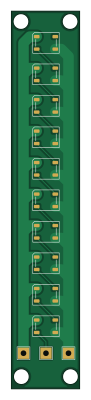
About the LED panel PCB
LED panel is an open source PCB design by HenryLi-0, published on GitHub under the Custom license license. It is a 2-layer board measuring 18 × 99.9 mm, with 10 components from 1 distinct parts.
It belongs with the displays & leds designs in this gallery.
From the project
A spinning LED light display! (Made for Hack Club's Highway YSWS!)
Checkout these folders!: - LED Subsystem - for the LED display logic (lots of LEDs!) - Motor Subsystem - for the logic and power controlling the motor (lots of power!) - LED Panel - for the LED Panel (this is made 5 times!)
LED panel bill of materials (BOM)
10 components, 1 distinct parts — part numbers from the project's BOM.
| Qty | Part | Footprint | Refs |
|---|---|---|---|
| 10 | WS2812B | LED_WS2812B_PLCC4_5.0x5.0mm_P3.2mm | D1, D2, D3, D4, D5, D6, D7, D8 +2 |
LED panel design files
The KiCad project lives in the HenryLi-0/raven repository on GitHub; these links point at the commit this page was built from.
LED panel: common questions
How big is the LED panel PCB?
The LED panel measures 18 × 99.9 mm, has 2 copper layers and is 1.6 mm thick.
How many components are on the LED panel?
10 components, from 1 distinct parts, with part numbers taken from the project's own BOM. The full bill of materials is listed on this page.
Where can I download the LED panel design files?
From the HenryLi-0/raven repository on GitHub, which has the KiCad layout, the schematic and the BOM; the links under Design files point to each one.
Can I use the LED panel design in my own project?
It is published under Custom license, which limits how it may be reused; read the license before building on it.
 atopile


 AxxAxx
 eez-open