
Snak 30 test

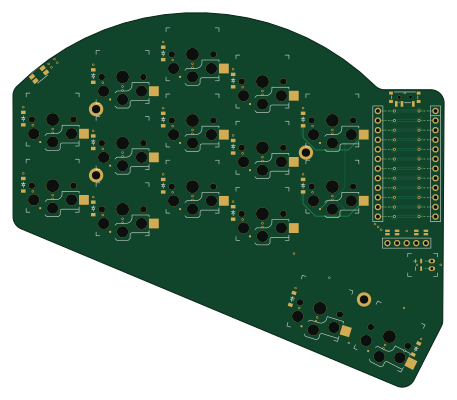
About the Snak 30 test PCB
Snak 30 test is an open source PCB design by JackMatanky, published on GitHub under the MIT license. It is a 2-layer board measuring 114 × 99 mm, with 7 components from 4 distinct parts.
It belongs with the keyboards, iot & wireless and displays & leds designs in this gallery.
From the project
SNAK (Sisyphus Needed a Keyboard): A split, low-profile, wireless keyboard designed with Ergogen and built with a nice!nano MCU, nice!view OLED, and Kailh choc switches
- The first version would not have been possible without flatfootfox's Let's Design a Keyboard With Ergogen guide. - Later versions were heavily inspired by ceolide's corney-island - Almost all footprints are from infused-kim
Snak 30 test bill of materials (BOM)
7 components, 4 distinct parts.
| Qty | Part | Footprint | Refs |
|---|---|---|---|
| 4 | — | mounting_hole | H1, H2, H3, H4 |
| 1 | — | JST_PH_S2B-PH-K | JST1 |
| 1 | — | power_switch | SW1 |
| 1 | — | sw_reset_side | SW2 |
Snak 30 test design files
The KiCad project lives in the JackMatanky/kb_snak repository on GitHub; these links point at the commit this page was built from.
Snak 30 test: common questions
How big is the Snak 30 test PCB?
The Snak 30 test measures 114 × 99 mm, has 2 copper layers and is 1.6 mm thick.
How many components are on the Snak 30 test?
7 components, from 4 distinct parts. The full bill of materials is listed on this page.
Where can I download the Snak 30 test design files?
From the JackMatanky/kb_snak repository on GitHub, which has the KiCad layout; the links under Design files point to each one.
Can I use the Snak 30 test design in my own project?
Yes, under the terms of its MIT license, which JackMatanky chose for the repository.
More boards in kb_snak
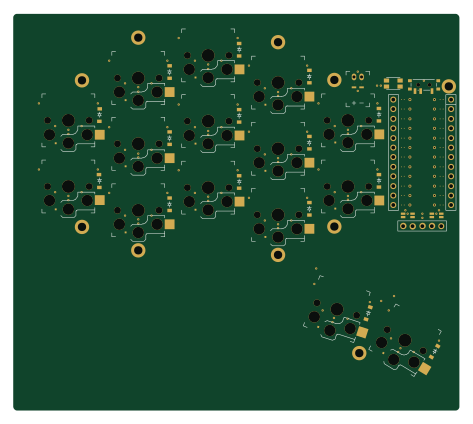
Snak 30 edge cuts
118.1 × 105 mm43 parts2LMIT1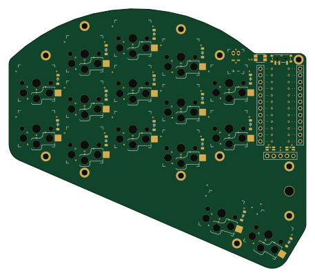
Snak 30
114 × 99.6 mm43 parts2LMIT1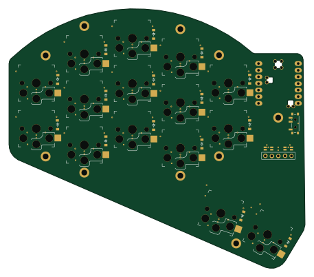 Nordic nRF
Snak 30 flatfoot
114 × 99.6 mm42 parts2LMIT1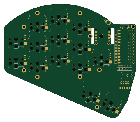
Snak 28 tp horizontal
114.8 × 99.6 mm42 parts2LMIT1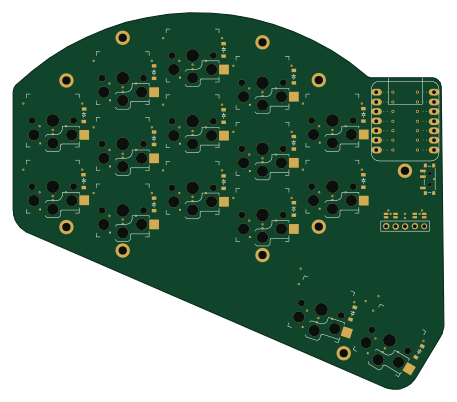
Snak 30 virginia
114 × 99.6 mm41 parts2LMIT1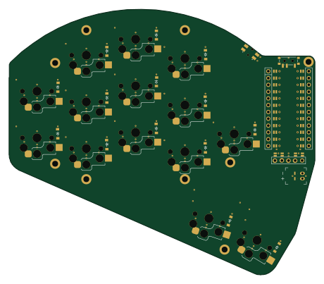
Snak 28 routing test
114.8 × 99.6 mm40 parts2LMIT1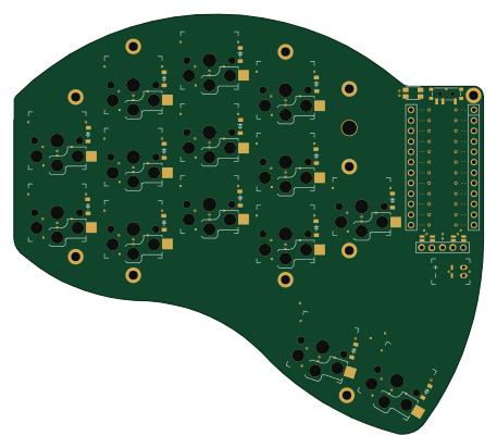
Snak 28 edge cuts
114 × 102.1 mm40 parts2LMIT1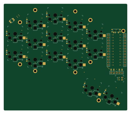
Snak 30 bottom border
114 × 98.5 mm13 parts2LMIT1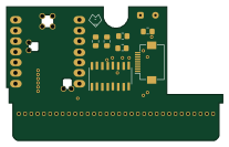 Nordic nRF
TypePak
51.7 × 32 mm10 parts2LMIT1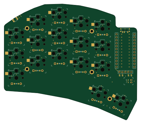
Snak test
114 × 99.4 mm8 parts2LMIT1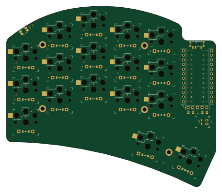
Snak final
114 × 98.8 mm8 parts2LMIT1
Similar boards
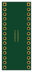
BM28B0.6-24DSBreakout
scottbez1
15.2 × 35.6 mm3 parts2LApache-2.022.2k
LevelShifterBreakout
15.2 × 20.3 mm5 parts2LApache-2.022.2k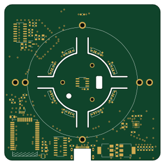
View base
81.2 × 81.2 mm81 parts2LApache-2.022.2k
View screen
35 × 35 mm12 parts2LApache-2.022.2k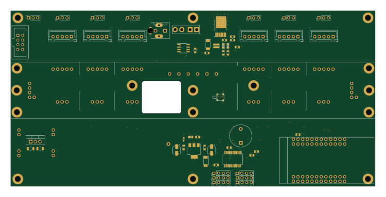
ChainlinkDriverTester
198.1 × 95.3 mm123 parts2LApache-2.04.2k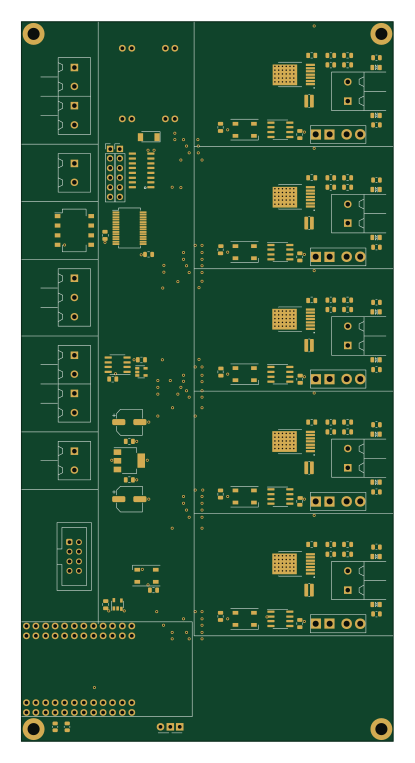
ChainlinkBase
98.4 × 190.5 mm119 parts2LApache-2.04.2k