Charging

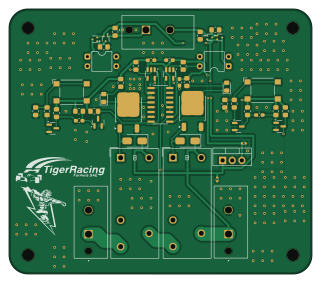
About the Charging PCB
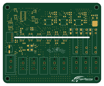
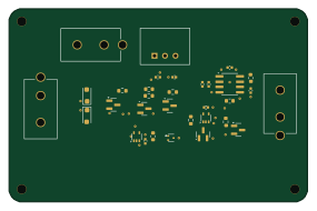
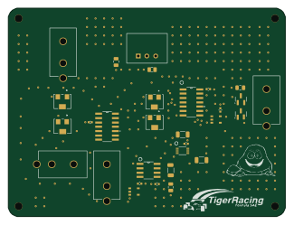
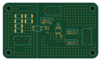
Charging is an open source PCB design by JacobParent7, published on GitHub. It is a 2-layer board measuring 80 × 70 mm, with 49 components from 20 distinct parts.
Other key parts include the SFH617A-1, 74AHC1G00, 74LS279 and LM7805_TO220. By type, the board carries 18 resistors, 10 transistors, 7 capacitors, 6 ICs, 4 diodes and 2 relays.
From the project
Repository for Fault Latch, BSPB, TSIL (TSSI) , TSAL (RML),
Create a token in github so you can pull the repository in git bash
git clone https://github.com/JacobParent7/FSAE_ELECTRONICS.git
right click on FSAE_ELECTRONICS in git bash terminal to open file location and find KiCAD project
git commit -m "Description of work done in commit"
Main components on the Charging
Charging bill of materials (BOM)
49 components, 20 distinct parts — part numbers from the project's BOM.
| Qty | Part | Footprint | Refs |
|---|---|---|---|
| 2 | SFH617A-1 | DIP-4_W7.62mm | U1, U2 |
| 2 | 74AHC1G00 | SOT-23-5 | U3, U4 |
| 1 | 74LS279 | SOIC-16_3.9x9.9mm_P1.27mm | U5 |
| 1 | LM7805_TO220 | TO-220-3_Vertical | U107 |
| 2 | NMOS | TO-252-2 | Q1, Q2 |
| 4 | Q_PMOS_GSD | SOT-523_Custom(C96676) | Q101, Q102, Q107, Q108 |
| 4 | Q_NPN_BEC | SOT-23 | Q103, Q104, Q105, Q106 |
| 2 | RELAY_SPDT_OMRON_G2RL-1 Relay_SPDT_Omron_G2RL-1 | Relay_SPDT_Omron_G2RL-1 | K101, K102 |
| 2 | SW_OMRON_B3FS SW_Omron_B3FS | SW_SPST_Omron_B3FS-100xP | SW101, SW102 |
| 2 | LED | LED_0805_2012Metric_Pad1.15x1.40mm_HandSolder | D1, D2 |
| 2 | D_Schottky | D_SMA | D101, D102 |
| 3 | 100N 100n | C_0603_1608Metric_Pad1.08x0.95mm_HandSolder | C1, C2, C117 |
| 2 | 10N 10n | C_0603_1608Metric_Pad1.08x0.95mm_HandSolder | C101, C102 |
| 1 | 0.33U 0.33u | C_0402_1005Metric | C105 |
| 1 | 0.01U 0.01u | C_0402_1005Metric | C106 |
| 6 | 10K 10k | R_0805_2012Metric_Pad1.20x1.40mm_HandSolder | R1, R2, R5, R6, R105, R106 |
| 2 | 270 | R_0805_2012Metric_Pad1.20x1.40mm_HandSolder | R3, R4 |
| 5 | 1k | R_0805_2012Metric_Pad1.20x1.40mm_HandSolder | R101, R108, R109, R111, R113 |
| 1 | 2.2K | R_0805_2012Metric_Pad1.20x1.40mm_HandSolder | R102 |
| 4 | 100K 100k | R_0805_2012Metric_Pad1.20x1.40mm_HandSolder | R103, R104, R110, R112 |
Charging design files
The KiCad project lives in the JacobParent7/FSAE_ELECTRONICS repository on GitHub; these links point at the commit this page was built from.
Charging: common questions
How big is the Charging PCB?
The Charging measures 80 × 70 mm, has 2 copper layers and is 1.6 mm thick.
How many components are on the Charging?
49 components, from 20 distinct parts, with part numbers taken from the project's own BOM. The full bill of materials is listed on this page.
Where can I download the Charging design files?
From the JacobParent7/FSAE_ELECTRONICS repository on GitHub, which has the KiCad layout, the schematic and the BOM; the links under Design files point to each one.
Can I use the Charging design in my own project?
The repository has no license, so all rights stay with JacobParent7. Use it as a reference, and ask the author before reusing the design.