
Hackpad

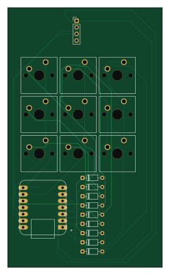
About the Hackpad PCB
Hackpad is an open source PCB design by javinwittig, published on GitHub. It is a 2-layer board measuring 59.5 × 100 mm, with 20 components from 4 distinct parts.
Other key parts include the MOUDLE-SEEEDUINO-XIAO. By type, the board carries 9 switches, 9 diodes, 1 IC and 1 connector.
It belongs with the keyboards and displays & leds designs in this gallery.
From the project
I made a custom 9-key macropad in a 3×3 layout, built with a Seeed Studio XIAO (SAMD21). Each switch has its own diode, wired as a 3×3 key matrix. It also features a small OLED display.
I made a custom 9-key macropad in a 3×3 layout, built with a Seeed Studio XIAO (SAMD21). Each switch has its own diode, wired as a 3×3 key matrix. It also features a small OLED display.
- 9 mechanical keys in a 3×3 grid where each has its own diode - Seeed Studio XIAO (SAMD21) as the controller - small OLED display - Custom KiCad PCB - Custom case modeled in Fusion 360, with cutouts for USB-C and the display header - Firmware based on KMK (CircuitPython)
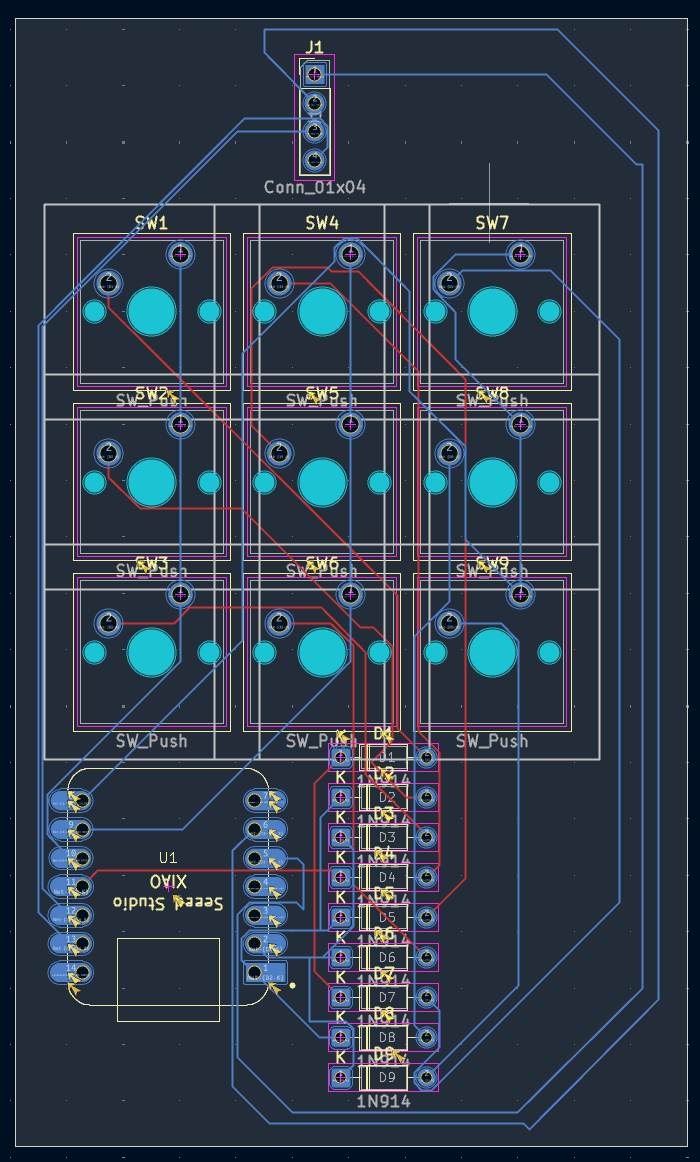
Main components on the Hackpad
Hackpad bill of materials (BOM)
20 components, 4 distinct parts.
| Qty | Part | Footprint | Refs |
|---|---|---|---|
| 1 | MOUDLE-SEEEDUINO-XIAO | XIAO-Generic-Hybrid-14P-2.54-21X17.8MM | U1 |
| 1 | Conn_01x04 | PinHeader_1x04_P2.54mm_Vertical | J1 |
| 9 | SW_Push | SW_Cherry_MX_1.00u_PCB | SW1, SW2, SW3, SW4, SW5, SW6, SW7, SW8 +1 |
| 9 | 1N914 | D_DO-35_SOD27_P7.62mm_Horizontal | D1, D2, D3, D4, D5, D6, D7, D8 +1 |
Hackpad design files
The KiCad project lives in the javinwittig/Hackpad repository on GitHub; these links point at the commit this page was built from.
Hackpad: common questions
How big is the Hackpad PCB?
The Hackpad measures 59.5 × 100 mm, has 2 copper layers and is 1.6 mm thick.
How many components are on the Hackpad?
20 components, from 4 distinct parts. The full bill of materials is listed on this page.
Where can I download the Hackpad design files?
From the javinwittig/Hackpad repository on GitHub, which has the KiCad layout and the schematic; the links under Design files point to each one.
Can I use the Hackpad design in my own project?
The repository has no license, so all rights stay with javinwittig. Use it as a reference, and ask the author before reusing the design.
Similar boards
BM28B0.6-24DSBreakout
scottbez1
15.2 × 35.6 mm3 parts2LApache-2.022.2k
View base
81.2 × 81.2 mm81 parts2LApache-2.022.2k
LevelShifterBreakout
15.2 × 20.3 mm5 parts2LApache-2.022.2k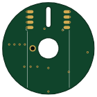
View screen
35 × 35 mm12 parts2LApache-2.022.2k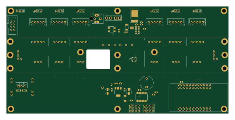
ChainlinkDriverTester
198.1 × 95.3 mm123 parts2LApache-2.04.2k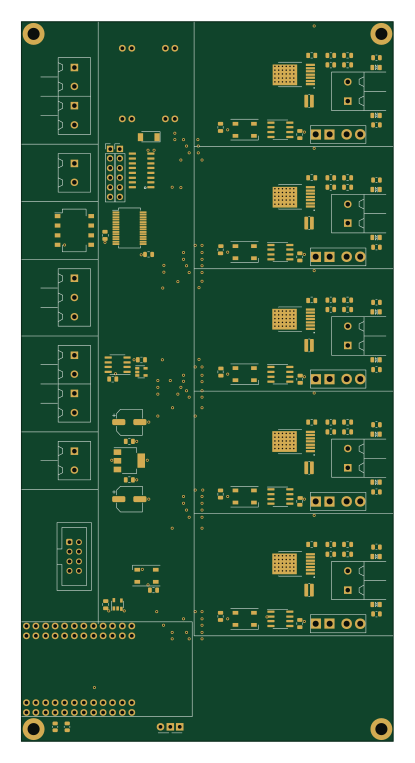
ChainlinkBase
98.4 × 190.5 mm119 parts2LApache-2.04.2k