
USB C BREAKOUT


About the USB C BREAKOUT
USB C BREAKOUT is an open source PCB design by jay94ks, published on GitHub under the MIT license. It is a 2-layer board measuring 17.5 × 13.7 mm, with 7 components from 6 distinct parts.
By type, the board carries 3 resistors, 2 connectors, 1 diode and 1 capacitor.
It belongs with the dev boards & breakouts designs in this gallery.
From the project
My own custom development boards
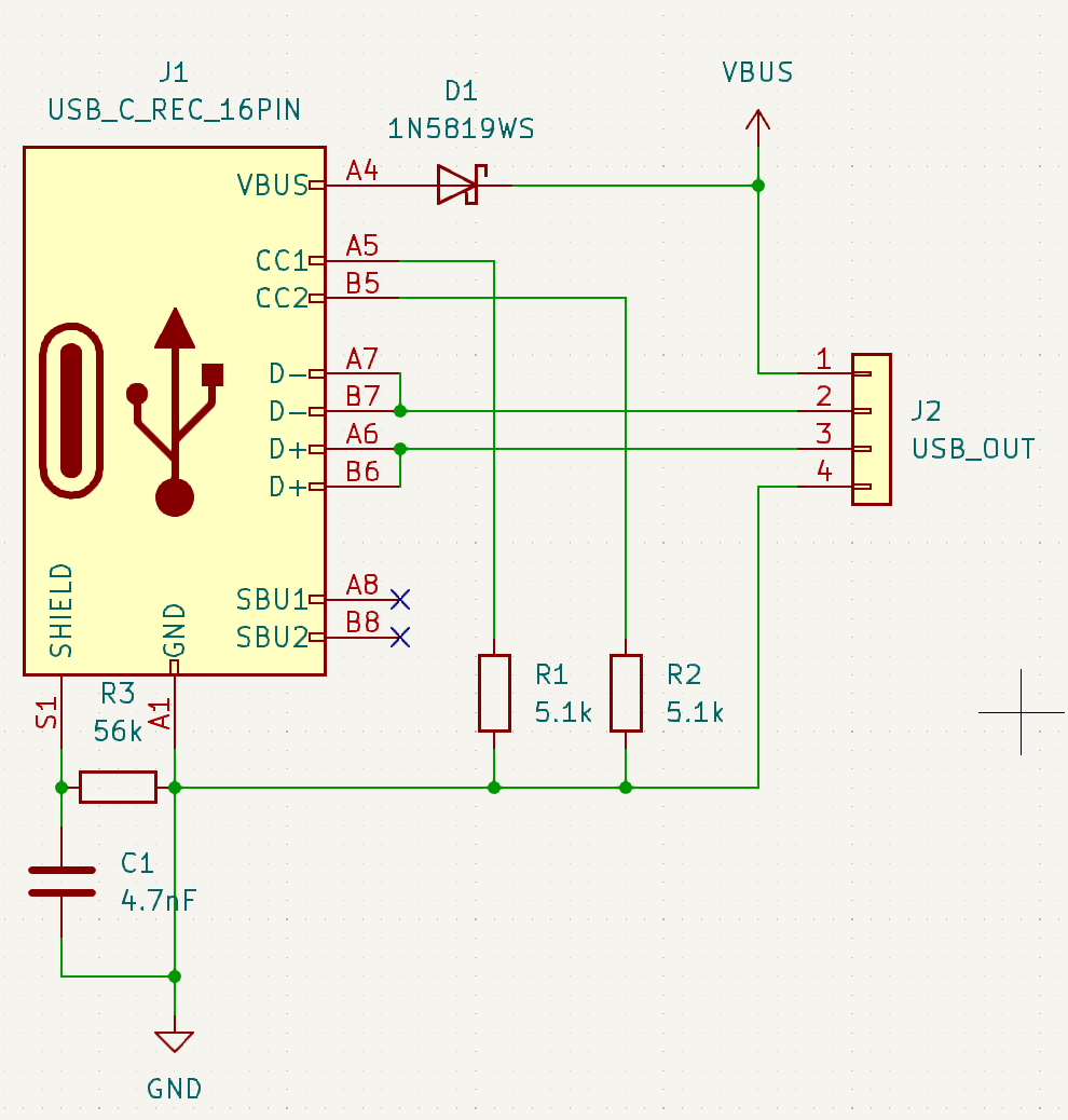
USB C BREAKOUT bill of materials (BOM)
7 components, 6 distinct parts.
| Qty | Part | Footprint | Refs |
|---|---|---|---|
| 1 | USB_C_REC_16PIN | USB_C_Receptacle_Palconn_UTC16-G | J1 |
| 1 | USB_OUT | PinHeader_1x04_P2.54mm_Horizontal | J2 |
| 1 | 1N5819WS | D_SOD-323_HandSoldering | D1 |
| 1 | 4.7nF | C_0603_1608Metric | C1 |
| 2 | 5.1k | R_0603_1608Metric | R1, R2 |
| 1 | 56k | R_0603_1608Metric | R3 |
USB C BREAKOUT design files
The KiCad project lives in the jay94ks/elecdev repository on GitHub; these links point at the commit this page was built from.
USB C BREAKOUT: common questions
How big is the USB C BREAKOUT?
The USB C BREAKOUT measures 17.5 × 13.7 mm, has 2 copper layers and is 1.6 mm thick.
How many components are on the USB C BREAKOUT?
7 components, from 6 distinct parts. The full bill of materials is listed on this page.
Where can I download the USB C BREAKOUT design files?
From the jay94ks/elecdev repository on GitHub, which has the KiCad layout and the schematic; the links under Design files point to each one.
Can I use the USB C BREAKOUT design in my own project?
Yes, under the terms of its MIT license, which jay94ks chose for the repository.
More boards in elecdev
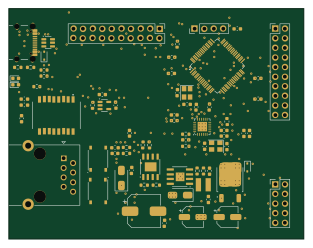 STM32
STM32F107RBT6
78.1 × 61 mm76 parts2LMIT0 RP2040/RP2350
RP2040 TB
40.6 × 51 mm50 parts2LMIT0 STM32
STM32F070F6P6
22.9 × 28.9 mm26 parts2LMIT0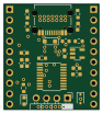 STM32
STM32F042F6P6
22.9 × 25.5 mm23 parts2LMIT0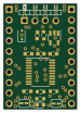 STM32
STM32G030F6P6
17.8 × 25.4 mm18 parts2LMIT0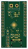 WCH CH32/CH55x
CH32X035G8U6
22.8 × 41.4 mm16 parts2LMIT0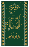 STM32
STM32G030K8T6
22.9 × 38.2 mm14 parts2LMIT0 RISC-V
CH32V003F4U6
18.2 × 25.5 mm11 parts2LMIT0 RISC-V
CH32V003F4P6
18.2 × 25.4 mm8 parts2LMIT0
Similar boards
134pin 7-967288-1
rusefi
139.7 × 73.7 mm38 parts2LGPL-3.01.2k
Breakout 112pin Connector
174 × 58 mm39 parts2LGPL-3.01.2k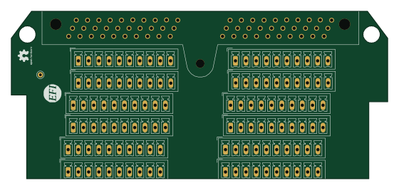
Breakout 60pin EEC-IV
139.7 × 62.2 mm15 parts2LGPL-3.01.2k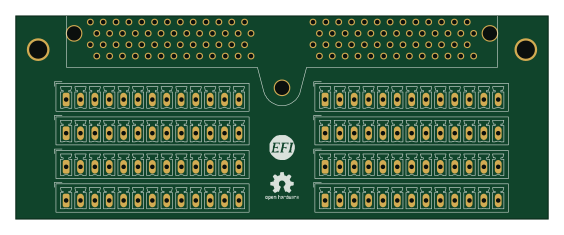
Eecv breakout
140.8 × 53.7 mm9 parts4LGPL-3.01.2k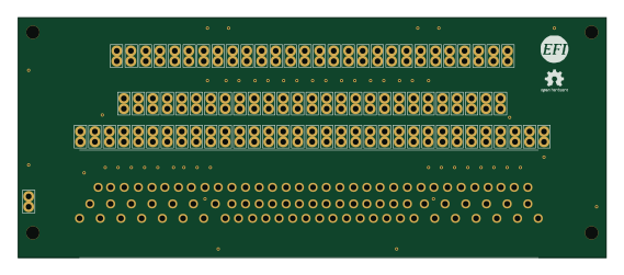
88 Pin Vag Breakout
142 × 58 mm91 parts2LGPL-3.01.2k
Rj45 breakout
rene-dev
15.2 × 53.8 mm3 parts2LGPL-3.0979