
ReBuster

About the ReBuster PCB
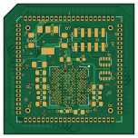
ReBuster is an open source FPGA PCB design by jbilander, published on GitHub under the CC-BY-SA-4.0 license. It is a 4-layer board measuring 38 × 38 mm, with 40 components from 17 distinct parts.
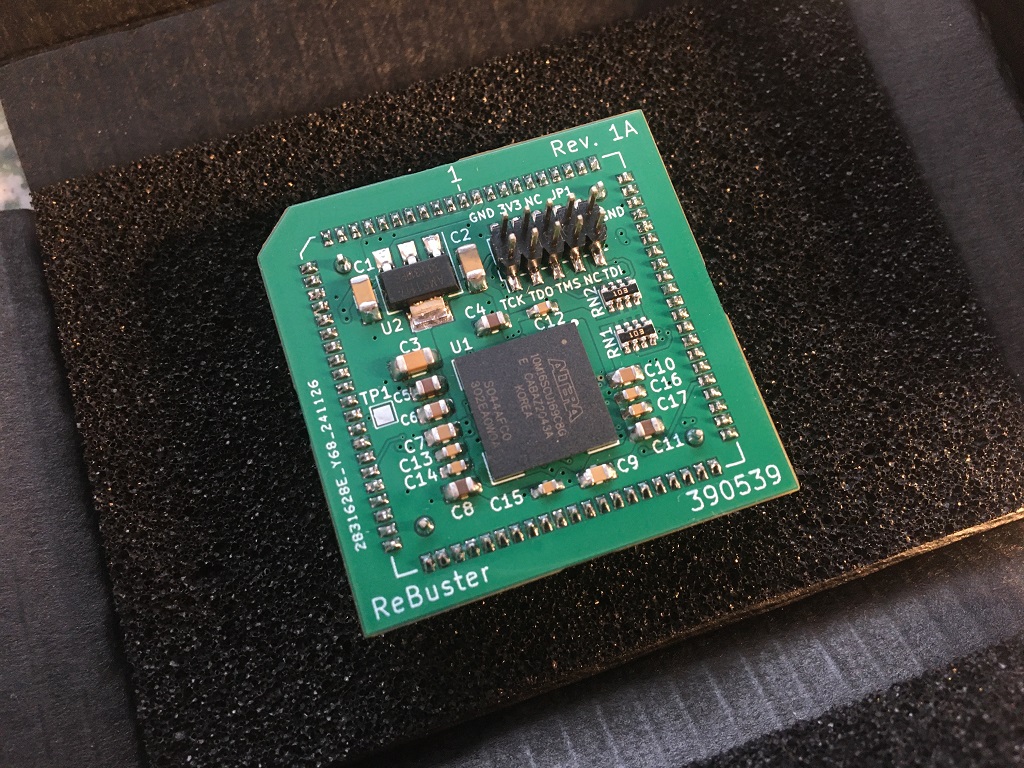
Its main chip is the 10M02SCU169, from the FPGA family. Other key parts include the LM1117-3.3, SN74CBTD16210, SN74LVC16245ADGVR, 74LVC2G07GV,125 and PLCC_84_plug. By type, the board carries 28 capacitors, 9 ICs and 2 resistors.
From the project
A drop in replacement PCB for the Super Buster chip
This is WORK IN PROGRESS. If you generate gerbers and order PCBs from this source you are doing so completely at your own risk!.
BOM Rev. 2A --------- Reference | Name/Value | Package | Notes -|-|-|-| U1 | 10M04SCU169C8G | BGA-169 11.0x11.0mmLayout13x13 | Max 10 FPGA 10M04SCU169C8G U2 | LM1117-3.3 | SOT-223 | Low-Dropout Linear Regulator 3.3 Volt U3,U5,U6 | SN74CBTD16210 | TSSOP-48 6.1x12.5mmP0.5mm | 20-BIT FET Bus switch with level shifting, high-speed TTL-compatible. 74CBTD16210DGGR U4 | SN74LVC16245ADGVR | TSSOP-484.4x9.7mmP0.4mm | 16-bit (dual-octal) noninverting bus transceiver…
Main components on the ReBuster
ReBuster bill of materials (BOM)
40 components, 17 distinct parts.
| Qty | Part | Footprint | Refs |
|---|---|---|---|
| 1 | 10M02SCU169 | BGA-169_11.0x11.0mm_Layout13x13_P0.8mm_Ball0.5mm_Pad0.35mm_NSMD | U1 |
| 1 | LM1117-3.3 | SOT-223 | U2 |
| 3 | SN74CBTD16210 | TSSOP-48_6.1x12.5mm_P0.5mm_padLength_1mm | U3, U5, U6 |
| 1 | SN74LVC16245ADGVR | TSSOP-48_4.4x9.7mm_P0.4mm_custom | U4 |
| 1 | 74LVC2G07GV,125 | TSOP-6_1.65x3.05mm_P0.95mm | U7 |
| 1 | PLCC_84_plug | PLCC-84_Plug_P1.27mm_mirrored | U8 |
| 1 | PLCC_84_plug | PLCC-84_TH_pin_holes | U9 |
| 1 | Conn_02x05_Odd_Even | PinHeader_2x05_P2.00mm_Vertical_SMD | JTAG1 |
| 3 | 10uF | C_1206_3216Metric_Pad1.42x1.75mm_HandSolder | C1, C2, C3 |
| 4 | 1uF | C_0805_2012Metric_Pad1.15x1.40mm_HandSolder | C4, C5, C8, C11 |
| 4 | 0.1uF | C_0805_2012Metric_Pad1.15x1.40mm_HandSolder | C6, C7, C9, C10 |
| 10 | 0.01uF | C_0603_1608Metric_Pad1.05x0.95mm_HandSolder | C12, C13, C14, C15, C16, C17, C19, C21 +2 |
| 1 | 0.01uF | C_0603_1608Metric | C18 |
| 1 | 0.1uF | C_0603_1608Metric_Pad1.05x0.95mm_HandSolder | C20 |
| 3 | 0.1uF | C_0603_1608Metric_Pad1.05x0.95mm_HandSolder_extended | C24, C25, C28 |
| 2 | 0.1uF | C_0603_1608Metric_Pad1.08x0.95mm_HandSolder | C26, C27 |
| 2 | 10k | RESCAF80P320X160X60-8N | RN1, RN2 |
ReBuster design files
The KiCad project lives in the jbilander/ReBuster repository on GitHub; these links point at the commit this page was built from.
- LayoutKiCad/ReBuster.kicad_pcb
ReBuster: common questions
What microcontroller does the ReBuster use?
The ReBuster is built around the 10M02SCU169, from the FPGA family.
How big is the ReBuster PCB?
The ReBuster measures 38 × 38 mm, has 4 copper layers and is 1.6 mm thick.
How many components are on the ReBuster?
40 components, from 17 distinct parts. The full bill of materials is listed on this page.
Where can I download the ReBuster design files?
From the jbilander/ReBuster repository on GitHub, which has the KiCad layout; the links under Design files point to each one.
Can I use the ReBuster design in my own project?
Yes, under the terms of its CC-BY-SA-4.0 license, which jbilander chose for the repository.
Can I test firmware for the ReBuster without the hardware?
Yes. HardLabs builds a simulation of the board from its netlist and BOM, so you can run and debug FPGA firmware against it before you order a PCB.
Similar boards
 FPGA
FPGABase board
GlasgowEmbedded
80 × 49 mm222 parts4L0BSD2.2k FPGA
FPGAThunderscope Rev5.3
EEVengers
122.5 × 103.5 mm817 parts6LMIT1.3k FPGA
FPGAUsb sniffer
ataradov
58.2 × 38.1 mm86 parts2LBSD-3-Clause1.3k FPGA
FPGATomu, I'm
theacodes
13 × 9.4 mm40 parts4LMIT1.1k FPGA
FPGAIcepi zero
cheyao
65 × 30 mm143 parts4LSHL-2.1828 FPGA
FPGASd2snes
mrehkopf
101.5 × 83 mm147 partsGPL-2.0717