
HackPad

About the HackPad PCB
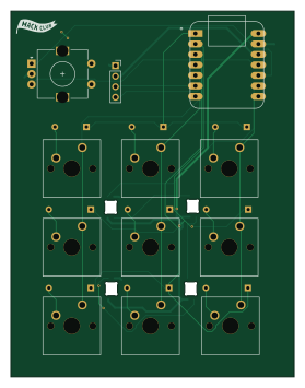
HackPad is an open source PCB design by jeshu-collab, published on GitHub. It is a 2-layer board measuring 68.5 × 88.5 mm, with 25 components from 7 distinct parts.
Other key parts include the MOUDLE-SEEEDUINO-XIAO. By type, the board carries 13 diodes, 10 switches, 1 IC and 1 connector.
It belongs with the keyboards and displays & leds designs in this gallery.
From the project
HackPad1 is a custom 9-key macropad built using the Seeed XIAO RP2040. It includes a rotary encoder, a 128x32 OLED display, and per-key RGB lighting. The firmware is written using KMK, making it easy to customize key mappings and add new features.
HackPad1 is a custom 9-key macropad built using the Seeed XIAO RP2040. It includes a rotary encoder, a 128x32 OLED display, and per-key RGB lighting. The firmware is written using KMK, making it easy to customize key mappings and add new features.
This project was designed from scratch, including the PCB, enclosure, and firmware.
- 9-key mechanical macropad (3x3 layout) - EC11 rotary encoder for volume control - 128x32 OLED display - Per-key RGB using SK6812MINI-E LEDs - Powered by Seeed XIAO RP2040 - KMK firmware for easy customization - Custom 2-piece 3D printed enclosure
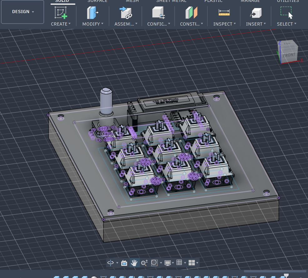
Main components on the HackPad
HackPad bill of materials (BOM)
25 components, 7 distinct parts — part numbers from the project's BOM.
| Qty | Part | Footprint | Refs |
|---|---|---|---|
| 1 | MOUDLE-SEEEDUINO-XIAO | XIAO-Generic-Hybrid-14P-2.54-21X17.8MM | U1 |
| 1 | CONN_01X04_PIN Conn_01x04_Pin | PinSocket_1x04_P2.54mm_Vertical | J1 |
| 9 | SW_Push | SW_Cherry_MX_1.00u_PCB | SW1, SW2, SW3, SW4, SW5, SW6, SW7, SW8 +1 |
| 1 | RotaryEncoder | RotaryEncoder_Alps_EC11E-Switch_Vertical_H20mm | SW10 |
| 3 | D | D_DO-35_SOD27_P7.62mm_Horizontal | D1, D2, D3 |
| 6 | D | D_DO-35_SOD27_P10.16mm_Horizontal | D4, D5, D6, D7, D8, D9 |
| 4 | WS2812B | MX_SK6812MINI-E | D10, D11, D12, D13 |
HackPad design files
The KiCad project lives in the jeshu-collab/HackPad repository on GitHub; these links point at the commit this page was built from.
- LayoutPCB/HackPad1.kicad_pcb
- SchematicPCB/HackPad1.kicad_sch
- BOMPCB/bom.csv
HackPad: common questions
How big is the HackPad PCB?
The HackPad measures 68.5 × 88.5 mm, has 2 copper layers and is 1.6 mm thick.
How many components are on the HackPad?
25 components, from 7 distinct parts, with part numbers taken from the project's own BOM. The full bill of materials is listed on this page.
Where can I download the HackPad design files?
From the jeshu-collab/HackPad repository on GitHub, which has the KiCad layout, the schematic and the BOM; the links under Design files point to each one.
Can I use the HackPad design in my own project?
The repository has no license, so all rights stay with jeshu-collab. Use it as a reference, and ask the author before reusing the design.
Similar boards
BM28B0.6-24DSBreakout
scottbez1
15.2 × 35.6 mm3 parts2LApache-2.022.2k
View base
81.2 × 81.2 mm81 parts2LApache-2.022.2k
LevelShifterBreakout
15.2 × 20.3 mm5 parts2LApache-2.022.2k
View screen
35 × 35 mm12 parts2LApache-2.022.2k
ChainlinkDriverTester
198.1 × 95.3 mm123 parts2LApache-2.04.2k
ChainlinkBase
98.4 × 190.5 mm119 parts2LApache-2.04.2k