
Neogeo diag aes prog

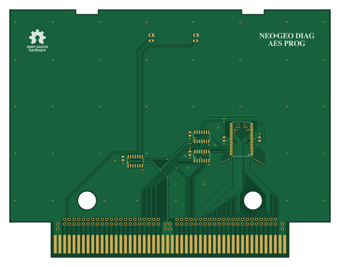
About the Neogeo diag aes prog PCB
Neogeo diag aes prog is an open source PCB design by jwestfall69, published on GitHub under the Unlicense license. It is a 2-layer board measuring 174 × 134 mm, with 17 components from 11 distinct parts.
Other key parts include the AS6C8016, 74LS08, 74LS11 and 74LS04. By type, the board carries 5 capacitors, 4 ICs, 4 connectors, 2 diodes and 2 resistors.
From the project
It works by using an SRAM chip instead of a ROM for the program rom on the PROG board. Doing this allows the diag bios to run tests on it similar to that of work ram to find issues.
It works by using an SRAM chip instead of a ROM for the program rom on the PROG board. Doing this allows the diag bios to run tests on it similar to that of work ram to find issues.
Its not possible to test all lines related to the program rom, so there are 2 leds at the top of the board. These 2 LEDs (ROMOE, PORTADDR) should be lit up when the P ROM Bus tests are running in the diag bios.
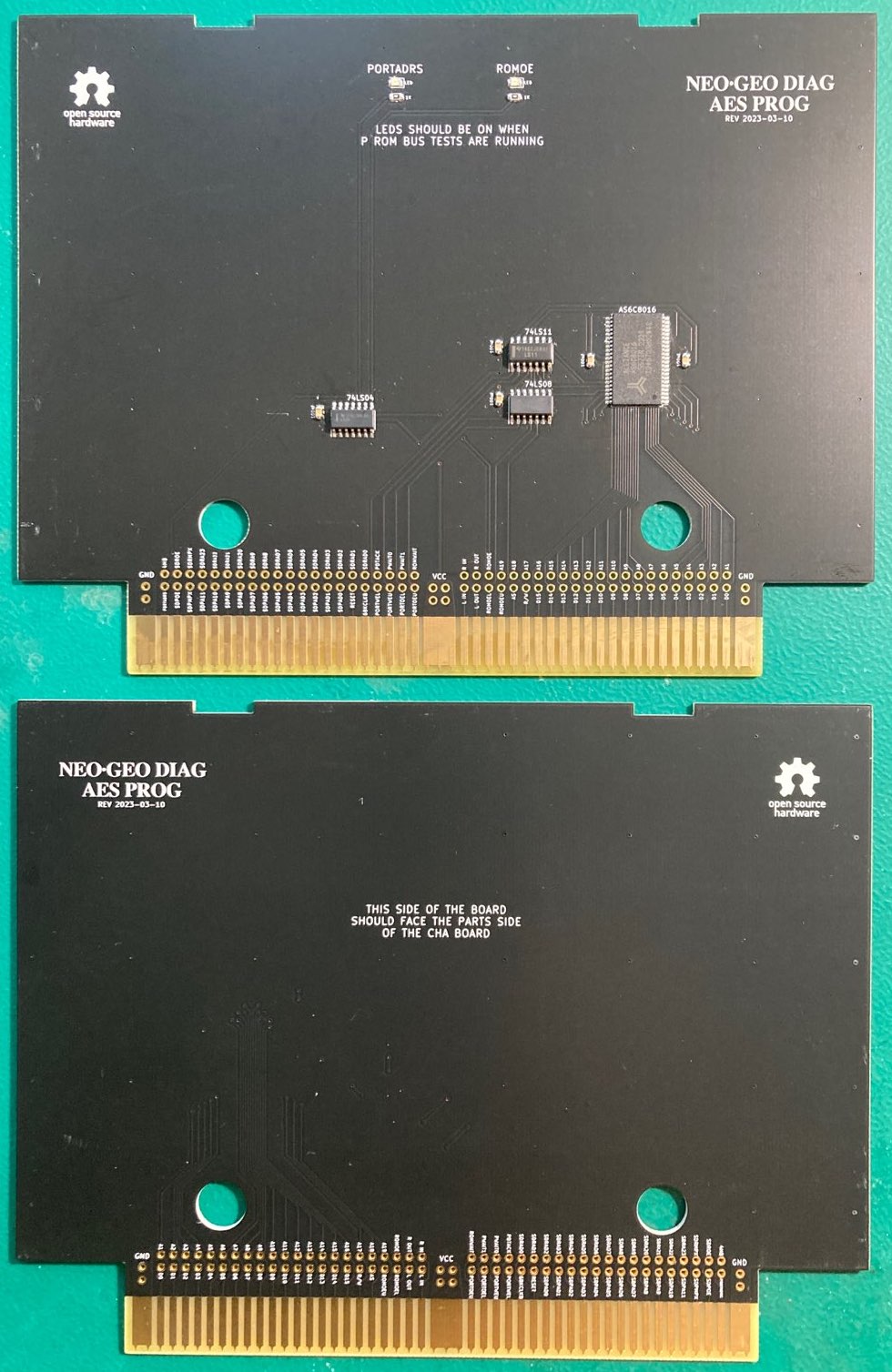
Main components on the Neogeo diag aes prog
Neogeo diag aes prog bill of materials (BOM)
17 components, 11 distinct parts.
| Qty | Part | Footprint | Refs |
|---|---|---|---|
| 1 | AS6C8016 | TSOP-II-44_10.16x18.41mm_P0.8mm | U1 |
| 1 | 74LS08 | SO-14_3.9x8.65mm_P1.27mm | U2 |
| 1 | 74LS11 | SO-14_3.9x8.65mm_P1.27mm | U3 |
| 1 | 74LS04 | SO-14_3.9x8.65mm_P1.27mm | U4 |
| 1 | neogeo-aes-prog-a-side-edge | neogeo-aes-prog-a-side-edge | J1 |
| 1 | neogeo-aes-prog-a-side-edge | neogeo-aes-prog-edge-test-points | J2 |
| 1 | neogeo-aes-prog-b-side-edge | neogeo-aes-prog-b-side-edge | J3 |
| 1 | neogeo-aes-prog-b-side-edge | neogeo-aes-prog-edge-test-points | J4 |
| 2 | LED | LED_0805_2012Metric | D1, D2 |
| 5 | 100nf | C_0805_2012Metric | C1, C2, C3, C4, C5 |
| 2 | 1K | R_0805_2012Metric | R1, R2 |
Neogeo diag aes prog design files
The KiCad project lives in the jwestfall69/neogeo-diag-aes-prog repository on GitHub; these links point at the commit this page was built from.
Neogeo diag aes prog: common questions
How big is the Neogeo diag aes prog PCB?
The Neogeo diag aes prog measures 174 × 134 mm, has 2 copper layers and is 1.6 mm thick.
How many components are on the Neogeo diag aes prog?
17 components, from 11 distinct parts. The full bill of materials is listed on this page.
Where can I download the Neogeo diag aes prog design files?
From the jwestfall69/neogeo-diag-aes-prog repository on GitHub, which has the KiCad layout and the schematic; the links under Design files point to each one.
Can I use the Neogeo diag aes prog design in my own project?
Yes, under the terms of its Unlicense license, which jwestfall69 chose for the repository.