
GPIO LADDER

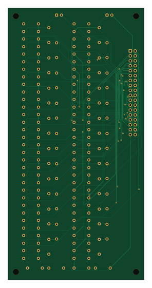
About the GPIO LADDER PCB
GPIO LADDER is an open source PCB design by k16shikano, published on GitHub. It is a 2-layer board measuring 70 × 140 mm, with 101 components from 3 distinct parts.
By type, the board carries 98 resistors, 2 capacitors and 1 connector.
From the project
16ビットR-2RラダーによるDAコンバーターの設計
- TOSリンク(S/PDIF)からの44.1kHz入力 - ノンオーバーサンプリング - 左右2チャンネル - カードケージ構成(同一回路を1枚にまとめた SINGLEBOARD` あり)
DACCHANNEL と DACCHANNELAXIAL は同一の電気設計**で、S3 / S5 のどちらにも挿さります。 ラダー抵抗の実装方法だけが違います。
SINGLEBOARD もカードケージと同一の電気設計です。JBP とバックプレーンは無く、 R チャネルは 8xxx 参照(U8001 など)。±VREF はチャネルごとにローカル生成のままです。 信号層は F.Cu / In2.Cu / In3.Cu / B.Cu、In1.Cu と In4.Cu が GND ベタ(ラダー下は抜き)。 JRAW ヘッダ(J401 / J402` およびチャネル側)は基板上配線のタップとして残しています。
GPIO LADDER bill of materials (BOM)
101 components, 3 distinct parts — part numbers from the project's BOM.
| Qty | Part | Footprint | Refs |
|---|---|---|---|
| 1 | 2x18 FEMALE from 2x FHU-1x42SG Akizuki 105779 | Socket_2x18_AB_Mating | J201 |
| 2 | 10UF 10uF | CP_Radial_D5.0mm_P2.50mm | C201, C301 |
| 98 | 10K 10k | R_Axial_DIN0207_L6.3mm_D2.5mm_P7.62mm_Horizontal | R201, R202, R203, R204, R205, R206, R207, R208 +90 |
GPIO LADDER design files
The KiCad project lives in the k16shikano/r2r-dac repository on GitHub; these links point at the commit this page was built from.
GPIO LADDER: common questions
How big is the GPIO LADDER PCB?
The GPIO LADDER measures 70 × 140 mm, has 2 copper layers and is 1.6 mm thick.
How many components are on the GPIO LADDER?
101 components, from 3 distinct parts, with part numbers taken from the project's own BOM. The full bill of materials is listed on this page.
Where can I download the GPIO LADDER design files?
From the k16shikano/r2r-dac repository on GitHub, which has the KiCad layout and the BOM; the links under Design files point to each one.
Can I use the GPIO LADDER design in my own project?
The repository has no license, so all rights stay with k16shikano. Use it as a reference, and ask the author before reusing the design.
More boards in r2r-dac
 Microchip SAM
SINGLE BOARD
175 × 150 mm349 parts6LNo license0 Microchip SAM
PANEL CARDS
300 × 308 mm234 parts4LNo license0
NOS R-2R DAC
75 × 154 mm122 parts4LNo license0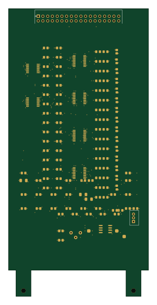
NOS R-2R DAC
75 × 154 mm122 parts4LNo license0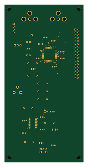 STM32
STM32GPIO CTRL
70 × 140 mm37 parts4LNo license0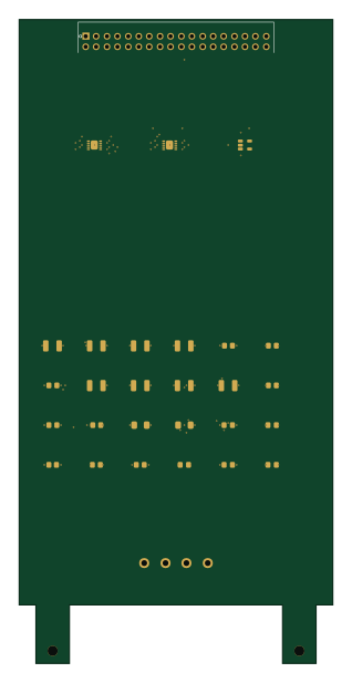
NOS R-2R DAC
75 × 154 mm29 parts4LNo license0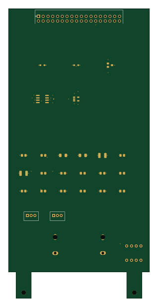
NOS R-2R DAC
75 × 154 mm29 parts4LNo license0
NOS R-2R DAC
75 × 154 mm24 parts4LNo license0 Microchip SAM
NOS R-2R DAC
75 × 154 mm19 parts4LNo license0
NOS R-2R DAC
250 × 75 mm7 parts4LNo license0
PANEL BACKPLANE
250 × 150 mm7 parts4LNo license0