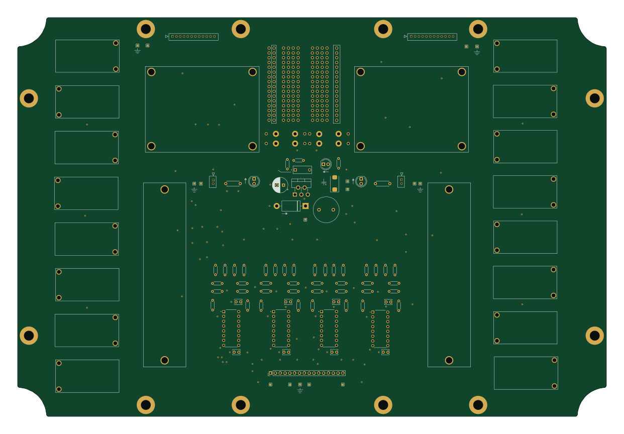
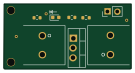
Mosfet chip panel

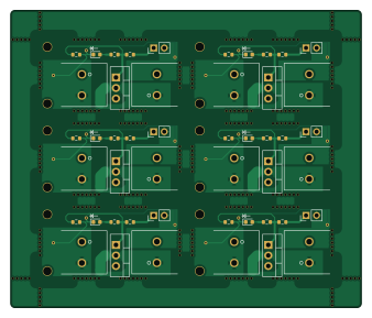
About the Mosfet chip panel PCB
Mosfet chip panel is an open source PCB design by kimballa, published on GitHub. It is a 2-layer board measuring 84.3 × 71.5 mm, with 8 components from 7 distinct parts.
By type, the board carries 3 connectors, 3 resistors, 1 transistor and 1 diode.
From the project
PCB Schematics for Like The Art project
You Don't Have to Like All the Art! -- PCBs ===========================================
PCB designs and eCAD files for the "You Don't Have to Like All the Art!" project.
This system consists of two distinct circuit boards:
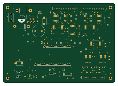
lta-logic-module - The "logic" that determines when it's dark out / should be active, what messages to light up on the sign, manages PWM or other effects when displaying the sign, and also handles button inputs from users. Runs on a combination of 5V and 3V3. This is designed around a port for installing an Adafruit Feather M4 Express (ATSAMD51 / Cortex-M4) Arduino…
Mosfet chip panel bill of materials (BOM)
8 components, 7 distinct parts — part numbers from the project's BOM.
| Qty | Part | Footprint | Refs |
|---|---|---|---|
| 1 | IRLZ34NPbF IRLZ34 Infineon | TO-220-3_Vertical | Q1 |
| 1 | 5-146858-1 Conn_01x02 | PinHeader_1x02_P2.54mm_Vertical | J1 |
| 2 | 1711725 Screw_Terminal_01x02 Phoenix Contact | Phoenix_1x02_1711725 | J2, J3 |
| 1 | XL-1608SURC-06 XINGLIGHT | LED_0603_1608Metric | D1 |
| 1 | 0603WAF1000T5E 100R UNI-ROYAL | R_0603_1608Metric | R1 |
| 1 | 0603WAF1002T5E 10K UNI-ROYAL | R_0603_1608Metric | R2 |
| 1 | 0603WAF3301T5E 3K3 UNI-ROYAL | R_0603_1608Metric | R3 |
Mosfet chip panel design files
The KiCad project lives in the kimballa/like-the-art-pcb repository on GitHub; these links point at the commit this page was built from.
Mosfet chip panel: common questions
How big is the Mosfet chip panel PCB?
The Mosfet chip panel measures 84.3 × 71.5 mm, has 2 copper layers and is 1.6 mm thick.
How many components are on the Mosfet chip panel?
8 components, from 7 distinct parts, with part numbers taken from the project's own BOM. The full bill of materials is listed on this page.
Where can I download the Mosfet chip panel design files?
From the kimballa/like-the-art-pcb repository on GitHub, which has the KiCad layout and the BOM; the links under Design files point to each one.
Can I use the Mosfet chip panel design in my own project?
The repository has no license, so all rights stay with kimballa. Use it as a reference, and ask the author before reusing the design.