
Patchwork devboard

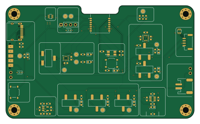
About the Patchwork devboard PCB
Patchwork devboard is an open source PCB design by KOUNOLAB, published on GitHub under the CERN-OHL-P-2.0 license. It is a 2-layer board measuring 100 × 60 mm, with 65 components from 22 distinct parts.
Other key parts include the C15879, C83224, C202311, C976032 and C6751361. By type, the board carries 23 resistors, 13 diodes, 11 capacitors, 8 switches, 7 ICs and 2 connectors.
It belongs with the dev boards & breakouts designs in this gallery.

Main components on the Patchwork devboard
Patchwork devboard bill of materials (BOM)
65 components, 22 distinct parts — part numbers from the project's BOM.
| Qty | Part | Footprint | Refs |
|---|---|---|---|
| 2 | C15879 SMF05CT1G | SOT65P210X110-6N | U1, U4 |
| 1 | C83224 M3406 | SOT-23-5 | U2 |
| 1 | C202311 BQ21040DBVR | SOT-23-6 | U3 |
| 1 | C976032 QMC5883L | LPCC-16 | U5 |
| 1 | C6751361 BC805M | XCVR_BC805M | U6 |
| 1 | C9900037528 LSM6DSV | Bosch_LGA-14_3x2.5mm_P0.5mm | U7 |
| 1 | N/A SWD_HEADER | PinHeader_1x04_P2.54mm_Vertical | J1 |
| 1 | C165948 USB_C_Receptacle_USB2.0 | USB_C_Receptacle_HRO_TYPE-C-31-M-12 | J2 |
| 6 | C2875122 SW_SPDT | MST-22D18G2 3J | SW1, SW2, SW3, SW6, SW7, SW8 |
| 2 | C318884 BUTTON | SW_Push_1P1T_XKB_TS-1187A | SW4, SW5 |
| 2 | C5178966 B5817WS | D_SOD-323 | D1, D2 |
| 10 | C2290 WHITE | LED_0603_1608Metric | D3, D4, D5, D7, D8, D9, D10, D11 +2 |
| 1 | C965844 RGB | LED_RGB_1210 | D6 |
| 1 | C1034 4.7uH | L_0603_1608Metric | L1 |
| 4 | C14663 100nF | C_0603_1608Metric | C1, C7, C10, C11 |
| 6 | C19666 4.7uF | C_0603_1608Metric | C2, C3, C4, C5, C6, C8 |
| 1 | C21120 220nF | C_0603_1608Metric | C9 |
| 2 | C23186 5k1 | R_0603_1608Metric | R1, R2 |
| 17 | C25804 10k | R_0603_1608Metric | R3, R5, R6, R7, R8, R10, R11, R12 +9 |
| 2 | C23178 470k | R_0603_1608Metric | R4, R18 |
Show 2 more
| Qty | Part | Footprint | Refs |
|---|---|---|---|
| 1 | C23137 330k | R_0603_1608Metric | R9 |
| 1 | C22976 2M | R_0603_1608Metric | R17 |
Patchwork devboard design files
The KiCad project lives in the KOUNOLAB/patchwork-devboard repository on GitHub; these links point at the commit this page was built from.
Patchwork devboard: common questions
How big is the Patchwork devboard PCB?
The Patchwork devboard measures 100 × 60 mm, has 2 copper layers and is 1.6 mm thick.
How many components are on the Patchwork devboard?
65 components, from 22 distinct parts, with part numbers taken from the project's own BOM. The full bill of materials is listed on this page.
Where can I download the Patchwork devboard design files?
From the KOUNOLAB/patchwork-devboard repository on GitHub, which has the KiCad layout, the schematic and the BOM; the links under Design files point to each one.
Can I use the Patchwork devboard design in my own project?
Yes, under the terms of its CERN-OHL-P-2.0 license, which KOUNOLAB chose for the repository.
Similar boards
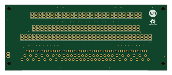
88 Pin Vag Breakout
rusefi
142 × 58 mm91 parts2LGPL-3.01.2k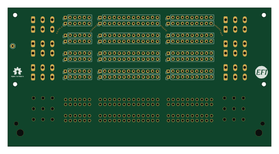
134pin 7-967288-1
139.7 × 73.7 mm38 parts2LGPL-3.01.2k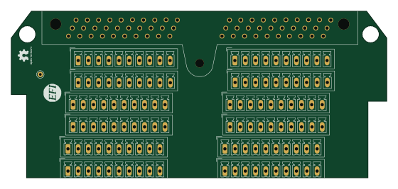
Breakout 60pin EEC-IV
139.7 × 62.2 mm15 parts2LGPL-3.01.2k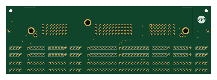
Breakout 112pin Connector
174 × 58 mm39 parts2LGPL-3.01.2k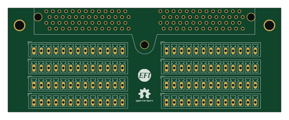
Eecv breakout
140.8 × 53.7 mm9 parts4LGPL-3.01.2k
Rj45 breakout
rene-dev
15.2 × 53.8 mm3 parts2LGPL-3.0979