
Sd breakout

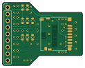
About the Sd breakout
Sd breakout is an open source PCB design by lbthomsen, published on GitHub under the Custom license license. It is a 2-layer board measuring 30.5 × 24.1 mm, with 10 components from 5 distinct parts.
By type, the board carries 6 resistors, 2 connectors and 2 capacitors.
It belongs with the dev boards & breakouts designs in this gallery.
From the project
SD Card Breakout Board
SD Card Breakout Board designed in KiCAD. Production files in the pcb directory.
Sd breakout bill of materials (BOM)
10 components, 5 distinct parts — part numbers from the project's BOM.
| Qty | Part | Footprint | Refs |
|---|---|---|---|
| 1 | MICRO_SD_CARD_DET2 Micro_SD_Card_Det2 | microSD_HC_Hirose_DM3D-SF | J1 |
| 1 | CONN_01X09 Conn_01x09 | PinHeader_1x09_P2.54mm_Vertical | J2 |
| 1 | 10UF 10uF | C_0603_1608Metric | C1 |
| 1 | 100NF 100nF | C_0603_1608Metric | C2 |
| 6 | 4K7 4k7 | R_0603_1608Metric | R1, R2, R3, R4, R5, R6 |
Sd breakout design files
The KiCad project lives in the lbthomsen/sd_breakout repository on GitHub; these links point at the commit this page was built from.
- Layoutpcb/sd.kicad_pcb
- Schematicpcb/sd.kicad_sch
- BOMpcb/sd_b_bom.csv
Sd breakout: common questions
How big is the Sd breakout?
The Sd breakout measures 30.5 × 24.1 mm, has 2 copper layers and is 1.2 mm thick.
How many components are on the Sd breakout?
10 components, from 5 distinct parts, with part numbers taken from the project's own BOM. The full bill of materials is listed on this page.
Where can I download the Sd breakout design files?
From the lbthomsen/sd_breakout repository on GitHub, which has the KiCad layout, the schematic and the BOM; the links under Design files point to each one.
Can I use the Sd breakout design in my own project?
It is published under Custom license, which limits how it may be reused; read the license before building on it.
Similar boards
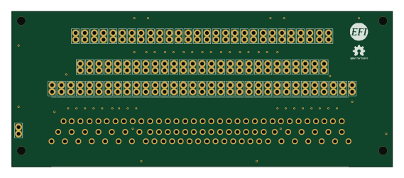
88 Pin Vag Breakout
rusefi
142 × 58 mm91 parts2LGPL-3.01.2k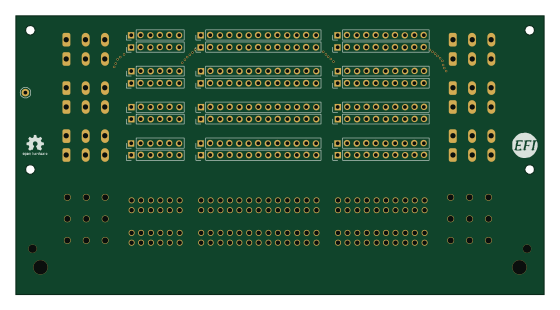
134pin 7-967288-1
139.7 × 73.7 mm38 parts2LGPL-3.01.2k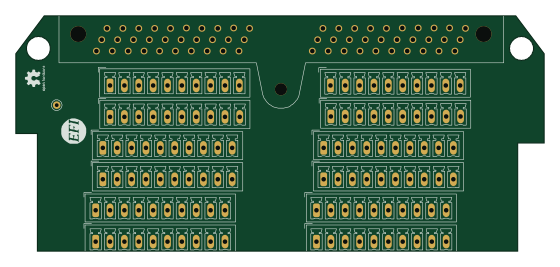
Breakout 60pin EEC-IV
139.7 × 62.2 mm15 parts2LGPL-3.01.2k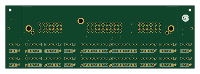
Breakout 112pin Connector
174 × 58 mm39 parts2LGPL-3.01.2k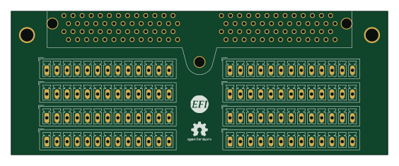
Eecv breakout
140.8 × 53.7 mm9 parts4LGPL-3.01.2k
Rj45 breakout
rene-dev
15.2 × 53.8 mm3 parts2LGPL-3.0979