
Fms link


About the Fms link PCB
Fms link is an open source PCB design by levicole, published on GitHub under the CC-BY-4.0 license. It is a 2-layer board measuring 15 × 27.9 mm, with 2 components from 2 distinct parts.
It belongs with the retro computing designs in this gallery.
From the project
A GB Link to 3.5mm adapter for syncing FMS with other devices (including Nanoloop)
A small PCB that plugs into a Game Boy link cable and breaks the sync lines out to a 3.5mm TRS jack, for clocking FMS and nanoloop against other gear — Pocket Operators, Volcas, eurorack, anything that takes an analog clock.
The previews are rendered bare, without the jack's 3D model, so the copper and silkscreen stay visible.
This matches the analog clock cable wiring in the FMS guide.
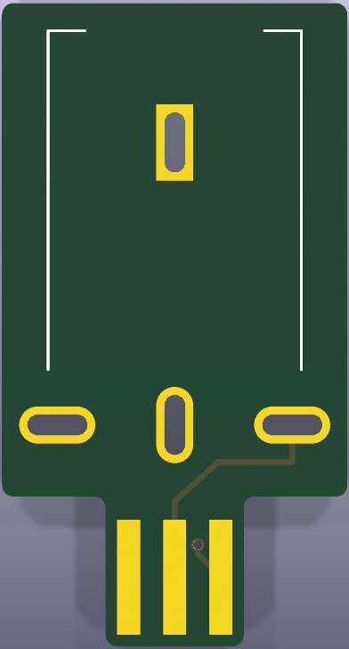
Fms link bill of materials (BOM)
2 components, 2 distinct parts — part numbers from the project's BOM.
| Qty | Part | Footprint | Refs |
|---|---|---|---|
| 1 | WQP-WQP729JH-B | Jack_3.5mm_QingPu_WQP-WQP729JH_Horizontal | J1 |
| 1 | gb-link-socket | gb-link-socket | GB1 |
Fms link design files
The KiCad project lives in the levicole/fms-link repository on GitHub; these links point at the commit this page was built from.
- Layoutfms-link.kicad_pcb
- Schematicfms-link.kicad_sch
- BOMReadme.md
Fms link: common questions
How big is the Fms link PCB?
The Fms link measures 15 × 27.9 mm, has 2 copper layers and is 1.6 mm thick.
How many components are on the Fms link?
2 components, from 2 distinct parts, with part numbers taken from the project's own BOM. The full bill of materials is listed on this page.
Where can I download the Fms link design files?
From the levicole/fms-link repository on GitHub, which has the KiCad layout, the schematic and the BOM; the links under Design files point to each one.
Can I use the Fms link design in my own project?
Yes, under the terms of its CC-BY-4.0 license, which levicole chose for the repository.
Similar boards
Amiga External
hoglet67
21.9 × 76.7 mm6 parts2LGPL-3.01.0k
Atari pickup
26.4 × 53.9 mm7 parts2LGPL-3.01.0k
Deniseadapter
26.7 × 62.2 mm16 parts2LGPL-3.01.0k
Analog
53.9 × 23.2 mm33 parts2LGPL-3.01.0k
Rgb to hdmi
77 × 97 mm67 parts2LGPL-3.01.0k
Buffer
53.9 × 23.2 mm13 parts2LGPL-3.01.0k