
IO

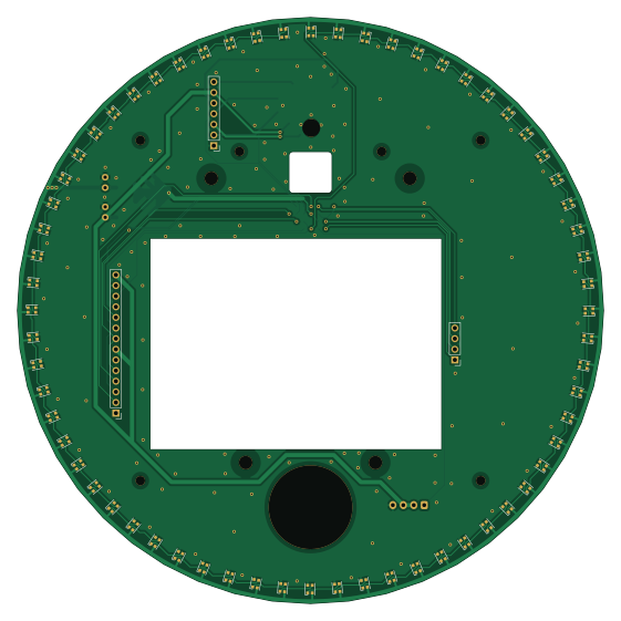
About the IO PCB
IO is an open source PCB design by MUNAKATA-EPC, published on GitHub. It is a 2-layer board measuring 140 × 140 mm, with 75 components from 10 distinct parts.
Other key parts include the AZ1084-3.3, AZ1084-5.0 and TWE-L-WX. By type, the board carries 64 diodes, 4 connectors, 4 capacitors and 3 ICs.
From the project
Munako Artemis 2025シーズンのリポジトリ
・PlatformIO等で作成されたプロジェクトフォルダの名前は (プロジェクト名)-(開発環境) にしましょう。 ex. hogehoge-teensy40 hugahuga-seeeduinoxiaorp2040
・KiCad、Fusion360などで作成されたフォルダ、ファイルの名前は一目でわかる名前にしましょう。
Main components on the IO
IO bill of materials (BOM)
75 components, 10 distinct parts.
| Qty | Part | Footprint | Refs |
|---|---|---|---|
| 1 | AZ1084-3.3 | TO-252-2 | U1 |
| 1 | AZ1084-5.0 | TO-252-2 | U2 |
| 1 | TWE-L-WX | MonoWireless_TWE-L-WX | U3 |
| 1 | Conn_01x14_Socket | PinHeader_1x14_P2.54mm_Vertical | J1 |
| 1 | Conn_01x04_Socket | JST_XH_B4B-XH-A_1x04_P2.50mm_Vertical | J2 |
| 1 | Conn_01x04_Socket | PinHeader_1x04_P2.54mm_Vertical | J3 |
| 1 | Conn_01x07_Socket | PinHeader_1x07_P2.54mm_Vertical | J5 |
| 64 | WS2812B | LED_WS2812B-2020_PLCC4_2.0x2.0mm | D1, D2, D3, D4, D5, D6, D7, D8 +56 |
| 2 | C | C_1210_3225Metric_Pad1.33x2.70mm_HandSolder | C1, C3 |
| 2 | C | C_Disc_D3.0mm_W1.6mm_P2.50mm | C2, C4 |
IO design files
The KiCad project lives in the MUNAKATA-EPC/Artemis_2025 repository on GitHub; these links point at the commit this page was built from.
IO: common questions
How big is the IO PCB?
The IO measures 140 × 140 mm, has 2 copper layers and is 1.6 mm thick.
How many components are on the IO?
75 components, from 10 distinct parts. The full bill of materials is listed on this page.
Where can I download the IO design files?
From the MUNAKATA-EPC/Artemis_2025 repository on GitHub, which has the KiCad layout and the schematic; the links under Design files point to each one.
Can I use the IO design in my own project?
The repository has no license, so all rights stay with MUNAKATA-EPC. Use it as a reference, and ask the author before reusing the design.
More boards in Artemis_2025
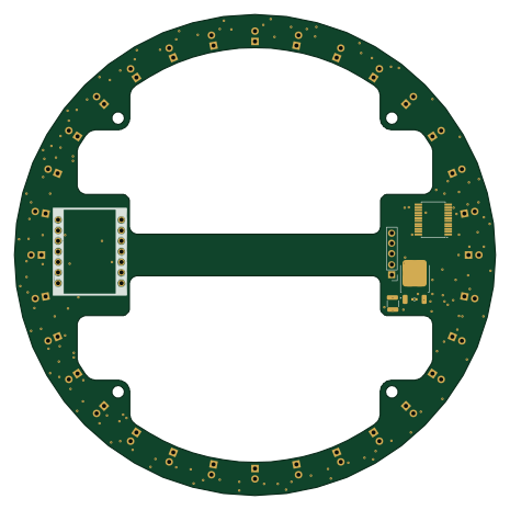
Line V2
116 × 116 mm86 parts2LNo license0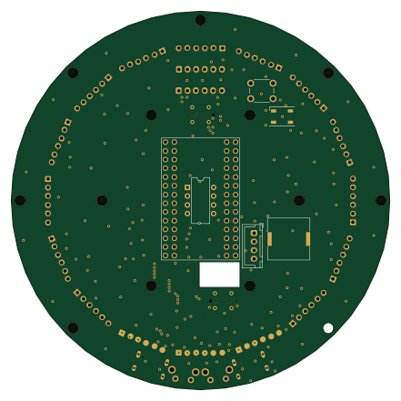 RP2040/RP2350
Main
110 × 110 mm61 parts2LNo license0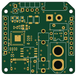 RP2040/RP2350
PSU
38 × 37.2 mm46 parts2LNo license0 RP2040/RP2350
MD
38 × 37.2 mm37 parts2LNo license0 NXP
CAM
85 × 78.7 mm29 parts2LNo license0
Kicker
38 × 37.2 mm22 parts2LNo license0
Relay
69.2 × 35 mm11 parts2LNo license0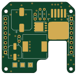
VoltageBooster
38 × 37.2 mm11 parts2LNo license0