
VoltageBooster

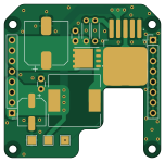
About the VoltageBooster PCB
VoltageBooster is an open source PCB design by MUNAKATA-EPC, published on GitHub. It is a 2-layer board measuring 38 × 37.2 mm, with 11 components from 9 distinct parts.
By type, the board carries 4 capacitors, 2 connectors, 2 resistors, 1 diode and 1 inductor.
From the project
Munako Artemis 2025シーズンのリポジトリ
・PlatformIO等で作成されたプロジェクトフォルダの名前は (プロジェクト名)-(開発環境) にしましょう。 ex. hogehoge-teensy40 hugahuga-seeeduinoxiaorp2040
・KiCad、Fusion360などで作成されたフォルダ、ファイルの名前は一目でわかる名前にしましょう。
VoltageBooster bill of materials (BOM)
11 components, 9 distinct parts.
| Qty | Part | Footprint | Refs |
|---|---|---|---|
| 2 | Conn_01x08_Socket | PinHeader_1x08_P2.54mm_Vertical | J1, J2 |
| 1 | XL6009 | TO-263-5_TabPin3 | VR1 |
| 1 | D | Infineon_PG-TDSON-8_6.15x5.15mm | D1 |
| 1 | 47μH | L_12x12mm_H6mm | L1 |
| 1 | 47μ | CP_Elec_6.3x5.9 | C1 |
| 2 | 0.1μ | C_Disc_D3.0mm_W1.6mm_P2.50mm | C2, C3 |
| 1 | 220μ | CP_Elec_10x10.5 | C4 |
| 1 | 47k | R_Axial_DIN0204_L3.6mm_D1.6mm_P5.08mm_Horizontal | R1 |
| 1 | 1k | R_Axial_DIN0204_L3.6mm_D1.6mm_P5.08mm_Horizontal | R2 |
VoltageBooster design files
The KiCad project lives in the MUNAKATA-EPC/Artemis_2025 repository on GitHub; these links point at the commit this page was built from.
VoltageBooster: common questions
How big is the VoltageBooster PCB?
The VoltageBooster measures 38 × 37.2 mm, has 2 copper layers and is 1.6 mm thick.
How many components are on the VoltageBooster?
11 components, from 9 distinct parts. The full bill of materials is listed on this page.
Where can I download the VoltageBooster design files?
From the MUNAKATA-EPC/Artemis_2025 repository on GitHub, which has the KiCad layout and the schematic; the links under Design files point to each one.
Can I use the VoltageBooster design in my own project?
The repository has no license, so all rights stay with MUNAKATA-EPC. Use it as a reference, and ask the author before reusing the design.
More boards in Artemis_2025
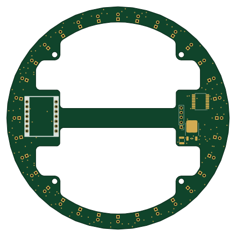
Line V2
116 × 116 mm86 parts2LNo license0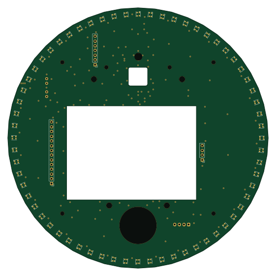
IO
140 × 140 mm75 parts2LNo license0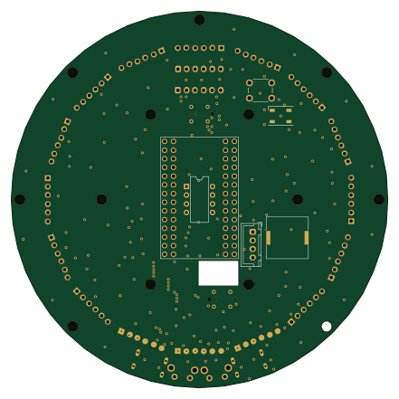 RP2040/RP2350
Main
110 × 110 mm61 parts2LNo license0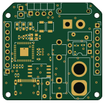 RP2040/RP2350
PSU
38 × 37.2 mm46 parts2LNo license0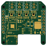 RP2040/RP2350
MD
38 × 37.2 mm37 parts2LNo license0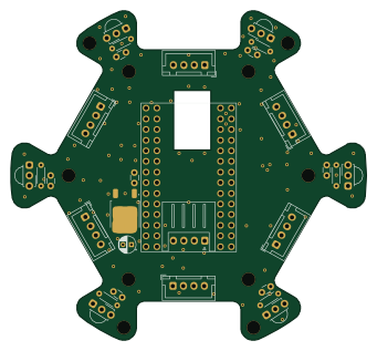 NXP
CAM
85 × 78.7 mm29 parts2LNo license0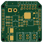
Kicker
38 × 37.2 mm22 parts2LNo license0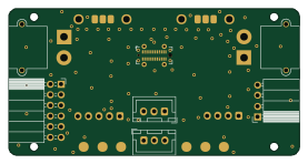
Relay
69.2 × 35 mm11 parts2LNo license0