
PCIe x8 Breakout

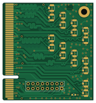
About the PCIe x8 Breakout
PCIe x8 Breakout is an open source PCB design by mwrnd, published on GitHub under the BSD-2-Clause license. It is a 4-layer board measuring 47.7 × 51.3 mm, with 42 components from 42 distinct parts.
By type, the board carries 36 connectors, 5 test points and 1 resistor.
It belongs with the dev boards & breakouts designs in this gallery.
From the project
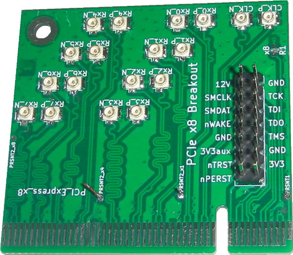
PCIe x8 Signal Breakout to U.FL/UMCC Connectors
PCIe x8 Signal Breakout to U.FL/UMCC Connectors.
PCIEX1-SMA is a similar project that is PCIe x1 and uses SMA connectors.
The board requires up to 34 U.FL/UMCC Surface Mount Receptacles and a 16-Pin 2.54mm Header or Socket.
Related Projects: OpenCAPIBreakout, OpenCAPI-to-PCIe, OpenCAPI-to-PCIex4Hostand_Endpoint
The board is currently being used along with an OpenCAPIBreakout board to test OpenCAPI-to-PCIe on the Innova-2 SmartNIC. PCIe 3.0 x4 at 8.0GT/s is currently working. Standard 0.1" M-F Jumpers are used for the PCIe Reset Signal (nPERST*) and its GND.
PCIe x8 Breakout bill of materials (BOM)
42 components, 42 distinct parts.
| Qty | Part | Footprint | Refs |
|---|---|---|---|
| 1 | PCI_Express_x8 | BUS_PCIexpress_x8 | J1 |
| 1 | Rx1_P | U.FL_Hirose_w_Label | J2 |
| 1 | Rx0_P | U.FL_Hirose_w_Label | J3 |
| 1 | Rx0_N | U.FL_Hirose_w_Label | J4 |
| 1 | Rx1_N | U.FL_Hirose_w_Label | J5 |
| 1 | Rx2_P | U.FL_Hirose_w_Label | J6 |
| 1 | Conn_02x08_Odd_Even | PinSocket_2x08_P2.54mm_Vertical | J7 |
| 1 | Rx2_N | U.FL_Hirose_w_Label | J8 |
| 1 | Rx3_P | U.FL_Hirose_w_Label | J9 |
| 1 | Rx3_N | U.FL_Hirose_w_Label | J10 |
| 1 | Rx4_P | U.FL_Hirose_w_Label | J11 |
| 1 | Rx4_N | U.FL_Hirose_w_Label | J12 |
| 1 | Rx5_P | U.FL_Hirose_w_Label | J13 |
| 1 | Rx5_N | U.FL_Hirose_w_Label | J14 |
| 1 | Rx6_P | U.FL_Hirose_w_Label | J15 |
| 1 | Rx6_N | U.FL_Hirose_w_Label | J16 |
| 1 | Rx7_P | U.FL_Hirose_w_Label | J17 |
| 1 | Rx7_N | U.FL_Hirose_w_Label | J18 |
| 1 | Tx0_P | U.FL_Hirose_w_Label | J19 |
| 1 | Tx0_N | U.FL_Hirose_w_Label | J20 |
Show 22 more
| Qty | Part | Footprint | Refs |
|---|---|---|---|
| 1 | Tx1_P | U.FL_Hirose_w_Label | J21 |
| 1 | Tx1_N | U.FL_Hirose_w_Label | J22 |
| 1 | Tx2_P | U.FL_Hirose_w_Label | J23 |
| 1 | Tx2_N | U.FL_Hirose_w_Label | J24 |
| 1 | Tx3_P | U.FL_Hirose_w_Label | J25 |
| 1 | Tx3_N | U.FL_Hirose_w_Label | J26 |
| 1 | Tx4_P | U.FL_Hirose_w_Label | J27 |
| 1 | Tx4_N | U.FL_Hirose_w_Label | J28 |
| 1 | Tx5_P | U.FL_Hirose_w_Label | J29 |
| 1 | Tx5_N | U.FL_Hirose_w_Label | J30 |
| 1 | Tx6_P | U.FL_Hirose_w_Label | J31 |
| 1 | Tx6_N | U.FL_Hirose_w_Label | J32 |
| 1 | Tx7_P | U.FL_Hirose_w_Label | J33 |
| 1 | Tx7_N | U.FL_Hirose_w_Label | J34 |
| 1 | CLK_P | U.FL_Hirose_w_Label | J35 |
| 1 | CLK_N | U.FL_Hirose_w_Label | J36 |
| 1 | GND | PinSocket_1x01_P2.54mm_Vertical | TP1 |
| 1 | PRSNT1 | PinHeader_1x01_P1.00mm_Vertical | TP6 |
| 1 | PRSNT2_x1 | PinHeader_1x01_P1.00mm_Vertical | TP7 |
| 1 | PRSNT2_x4 | PinHeader_1x01_P1.00mm_Vertical | TP8 |
| 1 | PRSNT2_x8 | PinHeader_1x01_P1.00mm_Vertical | TP9 |
| 1 | DNP | R_0603_1608Metric | R1 |
PCIe x8 Breakout design files
The KiCad project lives in the mwrnd/PCIe_x8_Breakout repository on GitHub; these links point at the commit this page was built from.
- LayoutPCIe_x8_Breakout.kicad_pcb
- SchematicPCIe_x8_Breakout.kicad_sch
PCIe x8 Breakout: common questions
How big is the PCIe x8 Breakout?
The PCIe x8 Breakout measures 47.7 × 51.3 mm, has 4 copper layers and is 1.6062 mm thick.
How many components are on the PCIe x8 Breakout?
42 components, from 42 distinct parts. The full bill of materials is listed on this page.
Where can I download the PCIe x8 Breakout design files?
From the mwrnd/PCIe_x8_Breakout repository on GitHub, which has the KiCad layout and the schematic; the links under Design files point to each one.
Can I use the PCIe x8 Breakout design in my own project?
Yes, under the terms of its BSD-2-Clause license, which mwrnd chose for the repository.
Similar boards
88 Pin Vag Breakout
rusefi
142 × 58 mm91 parts2LGPL-3.01.2k
134pin 7-967288-1
139.7 × 73.7 mm38 parts2LGPL-3.01.2k
Breakout 60pin EEC-IV
139.7 × 62.2 mm15 parts2LGPL-3.01.2k
Breakout 112pin Connector
174 × 58 mm39 parts2LGPL-3.01.2k
Eecv breakout
140.8 × 53.7 mm9 parts4LGPL-3.01.2k
Rj45 breakout
rene-dev
15.2 × 53.8 mm3 parts2LGPL-3.0979