
PS2 AT to USB Daughterboard for Leyden Jar controller

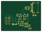
About the PS2 AT to USB Daughterboard for Leyden Jar controller PCB
PS2 AT to USB Daughterboard for Leyden Jar controller is an open source PCB design by mymakercorner, published on GitHub under the GPL-3.0 license. It is a 2-layer board measuring 35 × 26.5 mm, with 18 components from 15 distinct parts.
Other key parts include the LMV339 and USBLC6-2SC6. By type, the board carries 7 resistors, 3 capacitors, 2 ICs, 2 transistors, 2 connectors and 1 diode.
It belongs with the keyboards designs in this gallery.
From the project
A modernized controller PCB for the Brand New Model F and Beam Spring keyboards
The Leyden Jar is a modernized controller PCB for the Brand New Model F and Beam Spring keyboards. The name is taken from the first ever (crude) capacitor ever invented.
Please have a look at the Keebtalk here for more details on the development process. This repository is the central hub of several other repositories and links that may be need to build or dowloand software firmware and tools, see chapter below for more details.
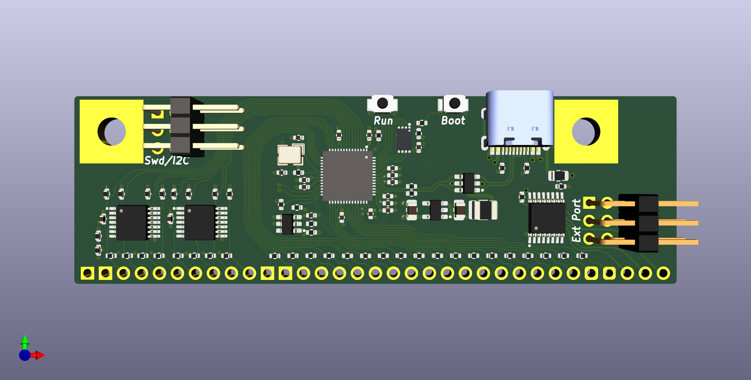
Main components on the PS2 AT to USB Daughterboard for Leyden Jar controller
PS2 AT to USB Daughterboard for Leyden Jar controller bill of materials (BOM)
18 components, 15 distinct parts — part numbers from the project's BOM.
| Qty | Part | Footprint | Refs |
|---|---|---|---|
| 1 | LMV339 MIC2009A-1YM6 | SOT-23-6 | U2 |
| 1 | USBLC6-2SC6 | SOT-23-6 | U3 |
| 2 | BSS138 | SOT-23 | Q1, Q2 |
| 1 | USB_C_RECEPTACLE_USB2.0 Conn_02x03_Odd_Even | PinSocket_2x03_P2.54mm_Horizontal | J1 |
| 1 | USB_C_Receptacle_USB2.0_16P | USB_C_Receptacle_HRO_TYPE-C-31-M-12 | J2 |
| 1 | D_Schottky_Small | D_SOD-123 | D1 |
| 1 | CBW201209U121T | R_805 | FB1 |
| 2 | 100N 1u | Capacitor_603 | C1, C5 |
| 1 | 100n | Capacitor_603 | C2 |
| 1 | 10K 1K | Resistor_603 | R1 |
| 1 | 2K | Resistor_603 | R2 |
| 1 | 1K | Resistor_603 | R3 |
| 2 | 1000 10K | Resistor_603 | R4, R5 |
| 1 | 10K | Resistor_603 | R6 |
| 1 | 47K 10K | Resistor_603 | R7 |
PS2 AT to USB Daughterboard for Leyden Jar controller design files
The KiCad project lives in the mymakercorner/Leyden_Jar repository on GitHub; these links point at the commit this page was built from.
PS2 AT to USB Daughterboard for Leyden Jar controller: common questions
How big is the PS2 AT to USB Daughterboard for Leyden Jar controller PCB?
The PS2 AT to USB Daughterboard for Leyden Jar controller measures 35 × 26.5 mm, has 2 copper layers and is 1.6 mm thick.
How many components are on the PS2 AT to USB Daughterboard for Leyden Jar controller?
18 components, from 15 distinct parts, with part numbers taken from the project's own BOM. The full bill of materials is listed on this page.
Where can I download the PS2 AT to USB Daughterboard for Leyden Jar controller design files?
From the mymakercorner/Leyden_Jar repository on GitHub, which has the KiCad layout, the schematic and the BOM; the links under Design files point to each one.
Can I use the PS2 AT to USB Daughterboard for Leyden Jar controller design in my own project?
Yes, under the terms of its GPL-3.0 license, which mymakercorner chose for the repository.
More boards in Leyden_Jar
Similar boards
Board-DjinnPlate
tzarc
191 × 152.9 mm4 parts2LCERN-OHL-S-2.0988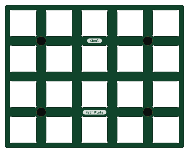
Half plate
95.3 × 76.2 mm24 parts2LCERN-OHL-S-2.0988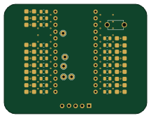
Mikoto flashbed
zhiayang
54 × 41.5 mm48 parts2LApache-2.0355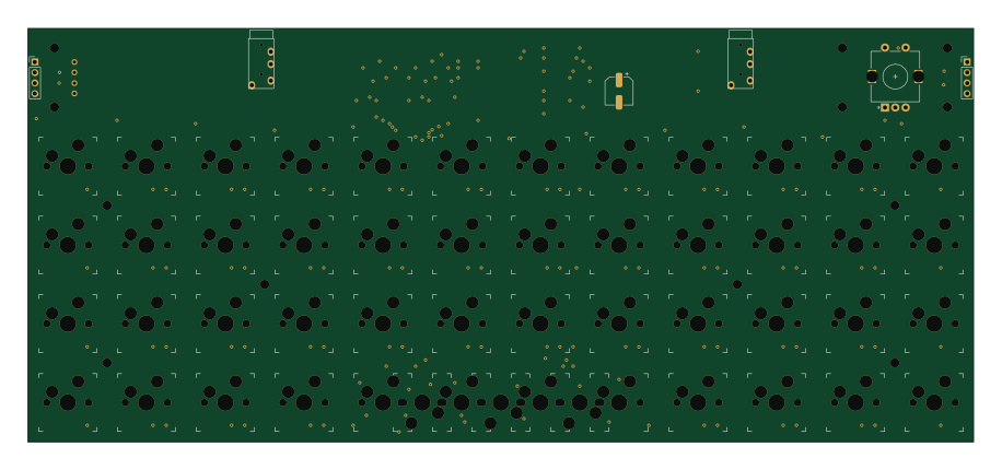
Mongus48
ChrisChrisLoLo
228.6 × 100 mm111 parts2LGPL-3.0334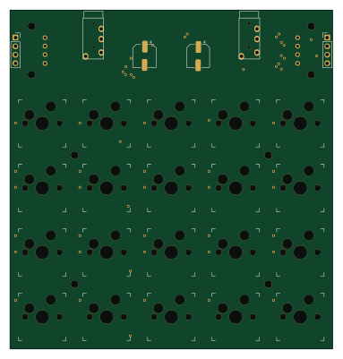
Beyblock20
95.3 × 100 mm51 parts2LGPL-3.0334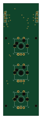
Knoblin3
31.8 × 100 mm11 parts2LGPL-3.0334