
Epc gain link

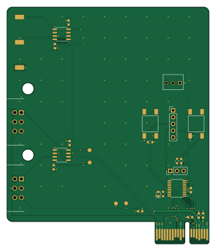
About the Epc gain link PCB
Epc gain link is an open source STM32 PCB design by oats-center, published on GitHub. It is a 4-layer board measuring 76.2 × 89.1 mm, with 27 components from 18 distinct parts.
Its main chip is the STM32G031F6P6, from the STM32 family. Other key parts include the TL072CDT. By type, the board carries 10 capacitors, 4 connectors, 3 ICs, 3 test points, 3 resistors and 2 switches.
From the project
Avena On The Road: Bringing pavement health data to your fingertips
Main components on the Epc gain link
Epc gain link bill of materials (BOM)
27 components, 18 distinct parts — part numbers from the project's BOM.
| Qty | Part | Footprint | Refs |
|---|---|---|---|
| 2 | TL072CDT TL072 | SO-8_3.9x4.9mm_P1.27mm | U1, U2 |
| 1 | STM32G031F6P6 STM32G031F6Px | TSSOP-20_4.4x6.5mm_P0.65mm | U3 |
| 1 | 1053866 Sensor2 | PC-1053866 | J1 |
| 1 | 1053866 Sensor1 | PC-1053866 | J3 |
| 1 | PZ2.54-S05P-A60 SWD | PinHeader_1x05_P2.54mm_Vertical | J4 |
| 1 | 3-641215-3 Link UART | TE_3-641215-3 | J5 |
| 1 | PZ2.54-S03P-A60 Forced Enable | PinHeader_1x03_P2.54mm_Vertical | JP1 |
| 1 | TS04-66-55-BK-260-SMT BOOT0 | SW_TS04-66-55-BK-260-SMT | SW1 |
| 1 | TS04-66-55-BK-260-SMT RESET | SW_TS04-66-55-BK-260-SMT | SW2 |
| 1 | 5017 GND | Keystone_5017 | TP4 |
| 1 | 5017 S1 | Keystone_5017 | TP8 |
| 1 | 5017 S2 | Keystone_5017 | TP9 |
| 1 | KT-0603B Status | D_0603_1608Metric | D1 |
| 2 | CGA0603X5R475K250JT 4u7 | C_0603_1608Metric | C1, C6 |
| 6 | CGA0603X7R104K500JT 100n | C_0603_1608Metric | C2, C4, C7, C8, C9, C10 |
| 2 | CGA0603X5R475K250JT 4.7u | C_0603_1608Metric | C3, C5 |
| 1 | RCA03270RFLF 270 | R_0603_1608Metric | R1 |
| 2 | RCA0310KJLF 10k | R_0603_1608Metric | R2, R3 |
Epc gain link design files
The KiCad project lives in the oats-center/avena-rs repository on GitHub; these links point at the commit this page was built from.
Epc gain link: common questions
What microcontroller does the Epc gain link use?
The Epc gain link is built around the STM32G031F6P6, from the STM32 family.
How big is the Epc gain link PCB?
The Epc gain link measures 76.2 × 89.1 mm, has 4 copper layers and is 1.6 mm thick.
How many components are on the Epc gain link?
27 components, from 18 distinct parts, with part numbers taken from the project's own BOM. The full bill of materials is listed on this page.
Where can I download the Epc gain link design files?
From the oats-center/avena-rs repository on GitHub, which has the KiCad layout, the schematic and the BOM; the links under Design files point to each one.
Can I use the Epc gain link design in my own project?
The repository has no license, so all rights stay with oats-center. Use it as a reference, and ask the author before reusing the design.
Can I test firmware for the Epc gain link without the hardware?
Yes. HardLabs builds a simulation of the board from its netlist and BOM, so you can run and debug STM32 firmware against it before you order a PCB.
More boards in avena-rs
 STM32
Link
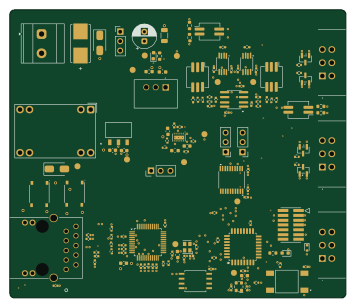
88.9 × 76.2 mm121 parts4LNo license3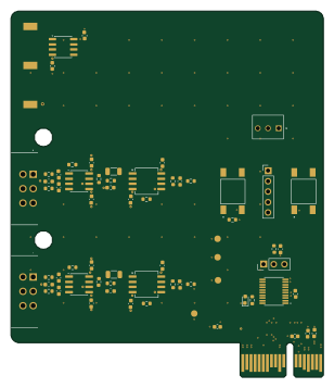 STM32
Sg gain link
76.2 × 89.1 mm64 parts4LNo license3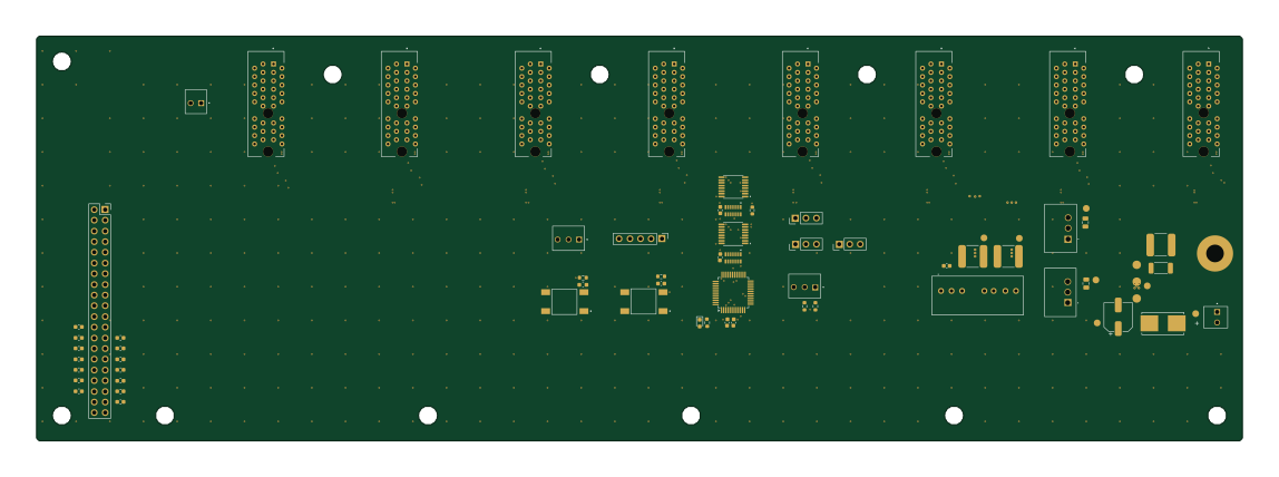 STM32
Mainboard
286.5 × 96.1 mm63 parts4LNo license3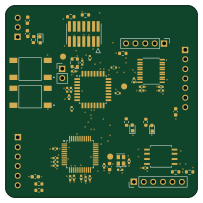 STM32
Controller
50.8 × 50.8 mm54 parts4LNo license3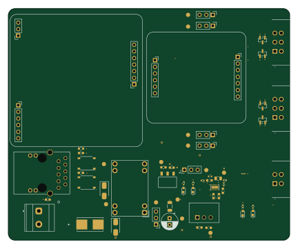
Motherboard
108 × 88.9 mm47 parts4LNo license3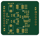
Signals
38.1 × 34.9 mm38 parts4LNo license3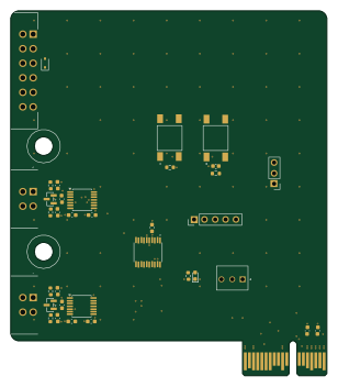 STM32
Tc link
76.2 × 87.8 mm36 parts4LNo license3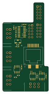 AVR/Arduino
Lattepanda breakout
39.4 × 76.2 mm26 parts4LNo license3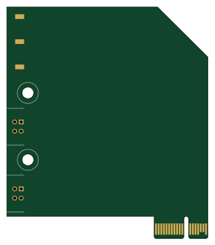
Link template
76.2 × 87.8 mm6 parts4LNo license3
Similar boards
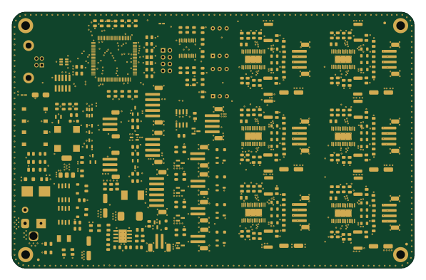 STM32
LumenPnP Motherboard
opulo-inc
149 × 95 mm296 parts4LCC-BY-SA-4.03.7k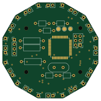 STM32
Base
google
52.3 × 52.3 mm36 parts2LApache-2.02.9k STM32
Type g
169 × 30 mm24 parts2LApache-2.02.9k STM32
Main panel
234 × 84 mm26 parts4LApache-2.02.9k STM32
Type a
150 × 30 mm14 parts2LApache-2.02.9k STM32
Type c
188 × 30 mm17 parts2LApache-2.02.9k