
Wafer keyboard v3

About the Wafer keyboard v3 PCB
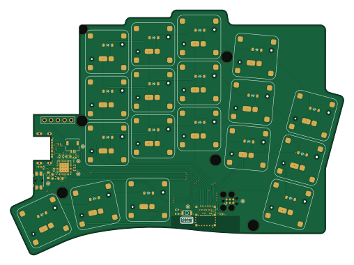
Wafer keyboard v3 is an open source PCB design by oleksandrmaslov, published on GitHub under the MIT license. It is a 6-layer board measuring 126.8 × 93.1 mm, with 122 components from 24 distinct parts.
Other key parts include the ISP1807-LR-RS, C94372 and C7501206. By type, the board carries 40 switches, 40 diodes, 18 capacitors, 10 resistors, 6 ICs and 4 connectors.
It belongs with the keyboards, robotics & motion and displays & leds designs in this gallery.
From the project
Wafer is the custom, ultra-thin mechanical keyboard built on nrf52840, with full NPM1300 integration and (custom spring) PG1316s switches. Built on ultra-efficient Zephyr and ZMK, has an integrated Memory-In-Pixel display, covered in a full CNC milled aluminum case, with only 4-8mm thin.
Wafer is a 36 key ultra-thin split keyboard that stays between 4–8 mm thick. It runs on an ISP1807 with an NPM1300 PMIC, and the full aluminium case snaps together with magnets for a clean profile. Runs ZMK for ultra-low-power
Default layout is shown above; layers and firmware live in this repo.
Here you could find the PCB and production files for the Wafer. There are two versions, with mousebites and ready for production and without them.
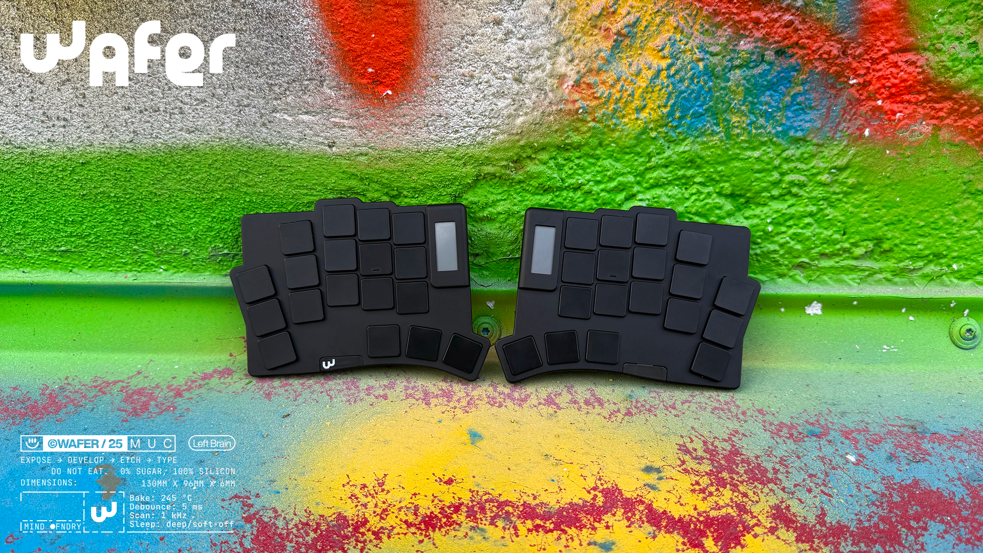
Main components on the Wafer keyboard v3
Wafer keyboard v3 bill of materials (BOM)
122 components, 24 distinct parts — part numbers from the project's BOM.
| Qty | Part | Footprint | Refs |
|---|---|---|---|
| 2 | ISP1807-LR-RS | ISP1807-LR-RS | U1, U6 |
| 2 | C94372 ESDR0502NMUTAG | UDFN-6_1.2x1.0mm_P0.4mm | U2, U4 |
| 2 | C7501206 nPM1300-QEXX | QFN-32-1EP_5x5mm_P0.5mm_EP3.6x3.6mm_ThermalVias | U3, U5 |
| 2 | C168688 USB_C_Receptacle_USB2.0 | USB-C_C168688 | J1, J4 |
| 2 | nice!view | display_nice_view | J3, J6 |
| 2 | Conn_01x02 | JST_SHL_SM02B-SHLS-TF_1x02-1MP_P1.00mm_Horizontal | Batt1, Batt2 |
| 36 | Keyswitch | CPG1316S01D02_front_mikefives | S1, S2, S3, S4, S5, S6, S7, S8 +28 |
| 2 | C963197 Reset | SW-SMD_L3.0-W2.0-LS3.5 | SW2, SW5 |
| 2 | C79174 Soft-off switch | Panasonic_EVQPUL_EVQPUC | SW3, SW6 |
| 36 | C466653 Diode | Diode_SOD-123 | D1, D2, D3, D4, D5, D6, D7, D8 +28 |
| 2 | C364554 RED | LED_0402_1005Metric | D19, D39 |
| 2 | C364550 BLUE | LED_0402_1005Metric | D20, D40 |
| 2 | MLZ2012A2R2WT000 2.2uH | L_0805_2012Metric | L1, L2 |
| 2 | C49062 100nF | C_0201_0603Metric | C1, C12 |
| 4 | C1691 10uF | C_0603_1608Metric | C2, C3, C13, C14 |
| 4 | C14445 1uF | C_0402_1005Metric | C4, C6, C15, C16 |
| 2 | CC0603KRX7R5BB105 10uF | C_0603_1608Metric | C7, C18 |
| 2 | CC0603KRX7R5BB105 1uF | C_0402_1005Metric | C8, C19 |
| 2 | CC0603KRX7R5BB105 2.2uF | C_0402_1005Metric | C9, C20 |
| 2 | C368809 4.7uF | C_0402_1005Metric | C10, C22 |
Show 4 more
| Qty | Part | Footprint | Refs |
|---|---|---|---|
| 2 | C25867 1.5k | R_0402_1005Metric | R1, R4 |
| 2 | C143981 150k | R_0201_0603Metric | R2, R9 |
| 2 | C114759 1.5k | R_0402_1005Metric | R3, R10 |
| 4 | C100126 10k | R_0201_0603Metric | R5, R6, R7, R8 |
Wafer keyboard v3 design files
The KiCad project lives in the oleksandrmaslov/wafer-zmk-config repository on GitHub; these links point at the commit this page was built from.
Wafer keyboard v3: common questions
How big is the Wafer keyboard v3 PCB?
The Wafer keyboard v3 measures 126.8 × 93.1 mm, has 6 copper layers and is 1.6 mm thick.
How many components are on the Wafer keyboard v3?
122 components, from 24 distinct parts, with part numbers taken from the project's own BOM. The full bill of materials is listed on this page.
Where can I download the Wafer keyboard v3 design files?
From the oleksandrmaslov/wafer-zmk-config repository on GitHub, which has the KiCad layout, the schematic and the BOM; the links under Design files point to each one.
Can I use the Wafer keyboard v3 design in my own project?
Yes, under the terms of its MIT license, which oleksandrmaslov chose for the repository.
More boards in wafer-zmk-config
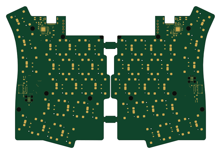
Similar boards
BM28B0.6-24DSBreakout
scottbez1
15.2 × 35.6 mm3 parts2LApache-2.022.2k
View base
81.2 × 81.2 mm81 parts2LApache-2.022.2k
LevelShifterBreakout
15.2 × 20.3 mm5 parts2LApache-2.022.2k
View screen
35 × 35 mm12 parts2LApache-2.022.2k
ChainlinkDriverTester
198.1 × 95.3 mm123 parts2LApache-2.04.2k
ChainlinkBase
98.4 × 190.5 mm119 parts2LApache-2.04.2k