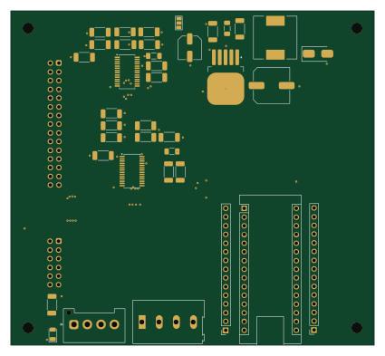
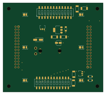
Fly High throughput - optogenetics

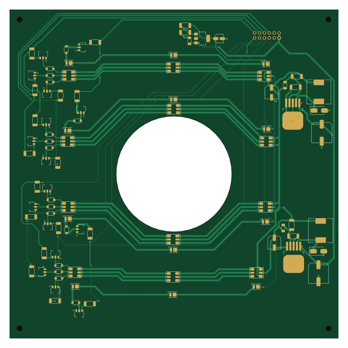
About the Fly High throughput - optogenetics PCB
Fly High throughput - optogenetics is an open source PCB design by open-neuroscience, published on GitHub under the GPL-3.0 license. It is a 2-layer board measuring 170 × 170 mm, with 94 components from 21 distinct parts.
Other key parts include the AL5809-150P1-7, AL5809-20P1-7, LM317_SOT-223 and LM2596S-ADJ. By type, the board carries 26 diodes, 22 resistors, 19 ICs, 16 transistors, 8 capacitors and 2 inductors.
From the project
In collaboration with BFKLAB, we are developing a system to measure behaviour of fruit flies. The system is high-throughput, that is, we can measure several animals at a time.
In collaboration with BFKLAB, we are developing a system to measure behaviour of fruit flies. The system is high-throughput, that is, we can measure several animals at a time.
The system will have interchangeable plates (round plates, narrow corridors) at the bottom, so different assays can be performed.
Other characteristics: - Vibration motors to disturb awake/sleep patterns - Bottom infrared illumination - RGB LEDs for Optogenetics - White LEDs for simulating day/night cycles
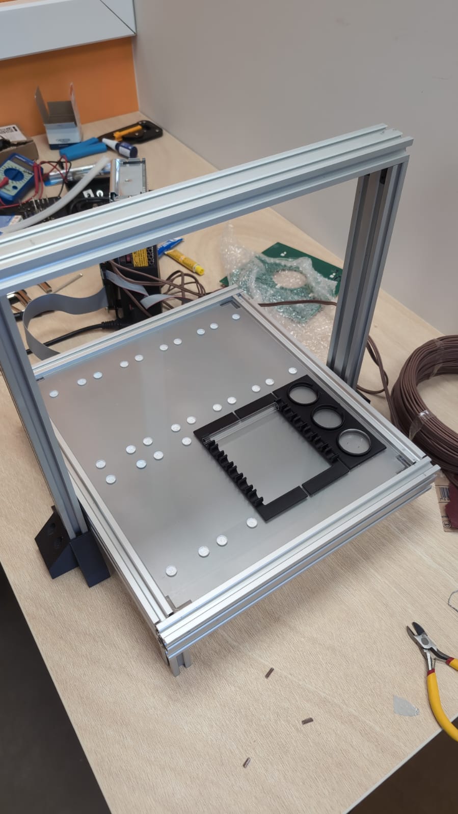
Main components on the Fly High throughput - optogenetics
Fly High throughput - optogenetics bill of materials (BOM)
94 components, 21 distinct parts — part numbers from the project's BOM.
| Qty | Part | Footprint | Refs |
|---|---|---|---|
| 12 | AL5809-150P1-7 | POWERDI123-C2_DIO-M | U1, U2, U3, U4, U5, U6, U7, U8 +4 |
| 4 | AL5809-20P1-7 | POWERDI123-C2_DIO-M | U13, U14, U15, U16 |
| 1 | LM317_SOT-223 | SOT-223-3_TabPin2 | U19 |
| 2 | LM2596S-ADJ | TO-263-5_TabPin3 | U21, U22 |
| 16 | C2923352 Q_NMOS_GDS | SOT-89-3 | Q1, Q2, Q3, Q4, Q5, Q6, Q7, Q8 +8 |
| 1 | CONN_02X06_ODD_EVEN Conn_02x06_Odd_Even | IDC-Header_2x06_P2.54mm_Horizontal | J1 |
| 12 | INOLUX_IN-P55TATRGB Inolux_IN-P55TATRGB | LED_Inolux_IN-P55TATRGB_PLCC6_5.0x5.5mm_P1.8mm | D1, D2, D3, D4, D5, D6, D7, D8 +4 |
| 12 | LED | LED_Everlight-SMD3528_3.5x2.8mm_67-21ST | D13, D14, D15, D16, D17, D18, D19, D20 +4 |
| 2 | C14651 Schottky 5A | D_SMB_Handsoldering | D25, D26 |
| 2 | C2929501 22µH | L_12x12mm_H4.5mm | L1, L2 |
| 1 | 0.1UF 0.1uF | C_1206_3216Metric_Pad1.33x1.80mm_HandSolder | C5 |
| 1 | 1UF 1uF | C_Elec_4x5.4 | C6 |
| 2 | C134782 680µF | C_Elec_10x10.2 | C9, C12 |
| 2 | 1.5NF 1.5nF | C_1206_3216Metric_Pad1.33x1.80mm_HandSolder | C10, C13 |
| 2 | C7469933 100µF | C_Elec_6.3x5.4 | C11, C14 |
| 16 | 220 | R_2010_5025Metric_Pad1.40x2.65mm_HandSolder | R1, R2, R3, R4, R5, R6, R7, R8 +8 |
| 1 | 2k | R_2010_5025Metric_Pad1.40x2.65mm_HandSolder | R21 |
| 1 | 540 | R_2010_5025Metric_Pad1.40x2.65mm_HandSolder | R22 |
| 1 | 3.9K 3.9k | R_2010_5025Metric_Pad1.40x2.65mm_HandSolder | R25 |
| 2 | 510 | R_2010_5025Metric_Pad1.40x2.65mm_HandSolder | R26, R28 |
Show 1 more
| Qty | Part | Footprint | Refs |
|---|---|---|---|
| 1 | 2.7K 2.7k | R_2010_5025Metric_Pad1.40x2.65mm_HandSolder | R27 |
Fly High throughput - optogenetics design files
The KiCad project lives in the open-neuroscience/Fly_highthroughput repository on GitHub; these links point at the commit this page was built from.
Fly High throughput - optogenetics: common questions
How big is the Fly High throughput - optogenetics PCB?
The Fly High throughput - optogenetics measures 170 × 170 mm, has 2 copper layers and is 1.6 mm thick.
How many components are on the Fly High throughput - optogenetics?
94 components, from 21 distinct parts, with part numbers taken from the project's own BOM. The full bill of materials is listed on this page.
Where can I download the Fly High throughput - optogenetics design files?
From the open-neuroscience/Fly_highthroughput repository on GitHub, which has the KiCad layout, the schematic and the BOM; the links under Design files point to each one.
Can I use the Fly High throughput - optogenetics design in my own project?
Yes, under the terms of its GPL-3.0 license, which open-neuroscience chose for the repository.