
P44ttngw

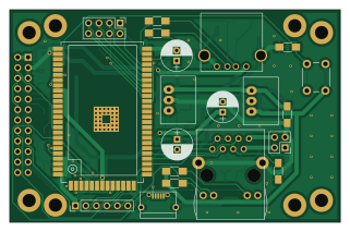
About the P44ttngw PCB
P44ttngw is an open source PCB design by plan44, published on GitHub. It is a 2-layer board measuring 80 × 51.4 mm, with 45 components from 21 distinct parts.
Other key parts include the ONION-OMEGA2S, R-78C5.0-1.0 and R_783.3-0.5. By type, the board carries 15 resistors, 13 capacitors, 7 diodes, 6 connectors, 3 ICs and 1 switch.
It belongs with the rf & radio designs in this gallery.
From the project
KiCAD files for TTN LoRA gateway based on RAK831 and Omega2S
This repository contains the KiCAD CAE files for a RAK831 + Omega2S based TTN LoRa gateway. This PCB can be sandwitched with a RAK831 LoRa concentrator board and fits into a 909060mm IP65 watertight Hammond 1554EGY enclosure.
The firmware for the project (a customized LEDE build) is contained in the plan of the plan44-feed LEDE feed repository in the p44ttngw-config package, see README there about how to build the firmware image from scratch.
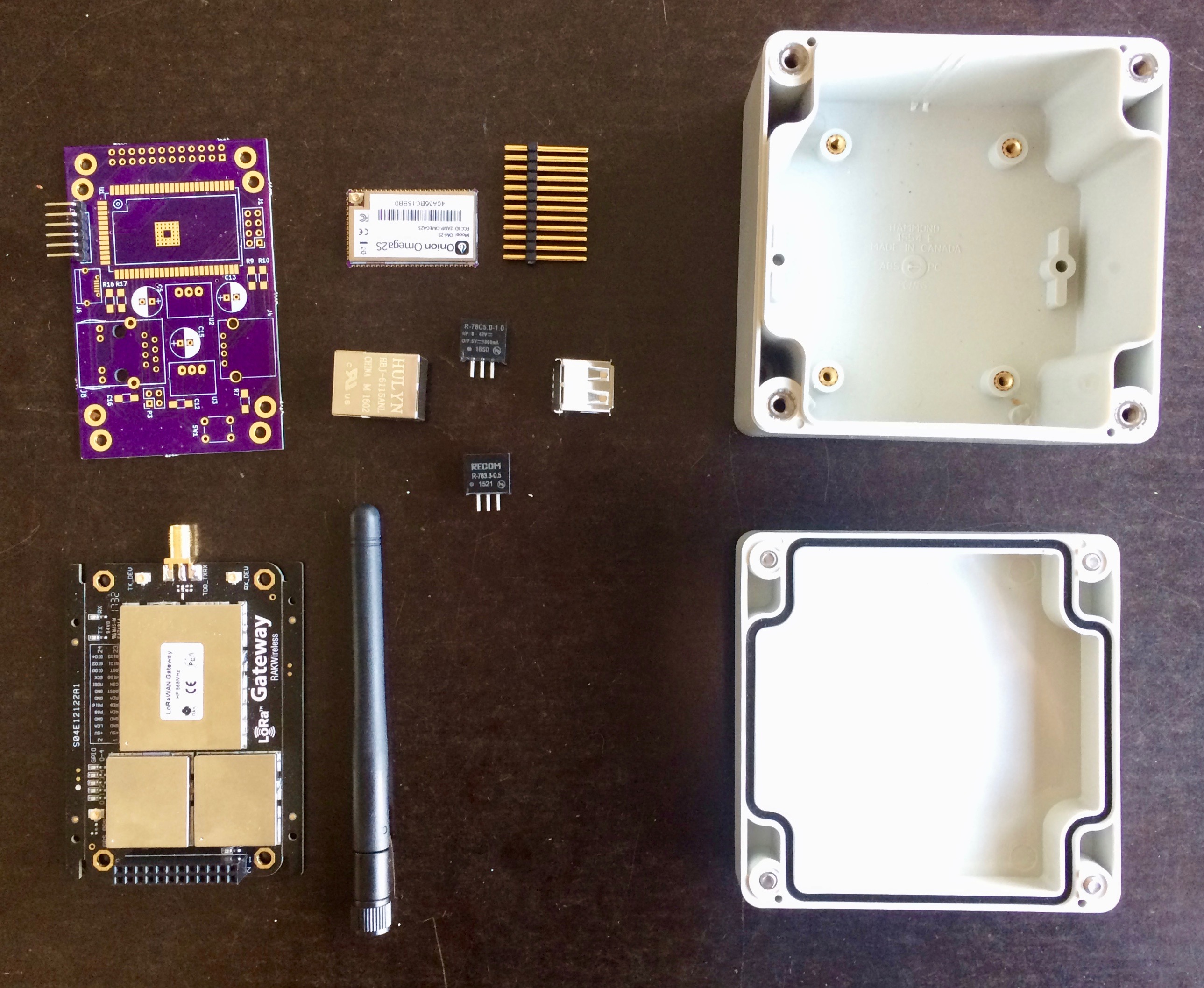
Main components on the P44ttngw
P44ttngw bill of materials (BOM)
45 components, 21 distinct parts.
| Qty | Part | Footprint | Refs |
|---|---|---|---|
| 1 | ONION-OMEGA2S | ONION-OMEGA2S | U1 |
| 1 | R-78C5.0-1.0 | Recom-R78Cxx | U2 |
| 1 | R_783.3-0.5 | Recom-R78Cxx | U3 |
| 1 | CONN_02X04 | Pin_Header_Straight_2x04_Pitch2.54mm | J1 |
| 1 | RAK831 | RAK831 | J3 |
| 1 | USB_A | USB_A | J4 |
| 1 | USB_Micro_AB | USB_Micro-B-SMD | J6 |
| 1 | FDI_Cable | Pin_Header_Straight_1x06_Pitch2.54mm | P1 |
| 1 | CONN_02X02 | Pin_Header_Straight_2x02_Pitch2.54mm | P3 |
| 1 | Omron PB | SW_PUSH_6mm_h4.3mm | SW1 |
| 3 | DO-214AA | D_SMB_Handsoldering | D2, D3, D4 |
| 4 | STPS1L30A | D_SMA_Handsoldering | D5, D6, D7, D8 |
| 9 | 100nF | C_1206_HandSoldering | C3, C4, C9, C10, C11, C12, C14, C17 +1 |
| 2 | 22uF 25V | CP_Radial_D7.5mm_P2.50mm | C5, C15 |
| 1 | 10uF 50VDC | CP_Radial_D7.5mm_P2.50mm | C13 |
| 1 | 1uF | C_1206_HandSoldering | C16 |
| 1 | 10k | R_1206_HandSoldering | R7 |
| 2 | 47R | R_1206_HandSoldering | R9, R10 |
| 4 | 49.9_1% | R_0805_HandSoldering | R11, R12, R13, R14 |
| 6 | 0R | R_1206_HandSoldering | R15, R18, R19, R20, R21, R22 |
Show 1 more
| Qty | Part | Footprint | Refs |
|---|---|---|---|
| 2 | 1k | R_1206_HandSoldering | R16, R17 |
P44ttngw design files
The KiCad project lives in the plan44/p44ttngw-hardware repository on GitHub; these links point at the commit this page was built from.
P44ttngw: common questions
How big is the P44ttngw PCB?
The P44ttngw measures 80 × 51.4 mm, has 2 copper layers and is 1.6 mm thick.
How many components are on the P44ttngw?
45 components, from 21 distinct parts. The full bill of materials is listed on this page.
Where can I download the P44ttngw design files?
From the plan44/p44ttngw-hardware repository on GitHub, which has the KiCad layout; the links under Design files point to each one.
Can I use the P44ttngw design in my own project?
The repository has no license, so all rights stay with plan44. Use it as a reference, and ask the author before reusing the design.
Similar boards
Hat
pa3gsb
65 × 56 mm81 parts2LNo license675
Radioberry juice
65 × 56 mm87 parts2LNo license675
Radioberry preamp
65 × 56 mm137 parts2LNo license675
Hermes-Lite Small IO Expansion
softerhardware
18.4 × 12.5 mm6 parts2LNo license372
Hermes-Lite Jumper With IO
21.9 × 51.7 mm12 parts2LNo license372
Hermes-Lite PureSignal Feedback
17.1 × 15.4 mm6 parts2LNo license372