
Testjig

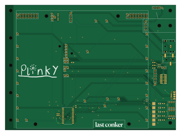
About the Testjig PCB
Testjig is an open source PCB design by plinkysynth, published on GitHub under the MIT license. It is a 2-layer board measuring 157.5 × 115.8 mm, with 79 components from 19 distinct parts.
Other key parts include the CD74HC4067M. By type, the board carries 53 connectors, 14 resistors, 7 diodes, 2 switches, 1 IC and 1 jumper.
From the project
a public release of the plinky sw and hw
the plinky testjig is a pcb that I made where I create two, and bolt them together with 5mm hex spacers, then solder pogopins (I forget the size! I got them on amazon lol) that poke thru to a plinky mainboard. https://www.youtube.com/watch?v=vNIF9_tz35w in THEORY someone could make one of these the advantage is that the jig can be used to flash plinky, and plinky detects that its mounted on a jig, and self calibrates all the AD/DA for cv control, and tests it, and you'll notice in the video a small 3d printed mount that allows you to place an OLED screen and so it tests all that. it also has…
Main components on the Testjig
Testjig bill of materials (BOM)
79 components, 19 distinct parts — part numbers from the project's BOM.
| Qty | Part | Footprint | Refs |
|---|---|---|---|
| 1 | CD74HC4067M | SOIC-24W_7.5x15.4mm_P1.27mm | U1 |
| 2 | Conn_02x08_Odd_Even | PinSocket_2x08_P2.54mm_Vertical | J1, J43 |
| 42 | Conn_01x01 | PinHeader_1x01_P2.54mm_Vertical | J2, J3, J4, J5, J6, J7, J8, J9 +34 |
| 3 | Conn_01x04_Female | PinSocket_1x04_P2.54mm_Vertical | J20, J46, J52 |
| 1 | C136000 USB_B_Micro | USB_Micro-B_Molex-105017-0001 | J44 |
| 1 | CONN_02X07_ODD_EVEN Conn_02x07_Odd_Even | PinHeader_2x07_P1.27mm_Vertical_SMD | J45 |
| 1 | Conn_01x06_Female | PinSocket_1x06_P2.54mm_Vertical | J47 |
| 1 | Conn_01x02_Female | PinSocket_1x02_P2.54mm_Vertical | J48 |
| 1 | SJ1-3523N-cap | CUI_SJ1-3523N | J51 |
| 1 | SJ1-3523N-CAP PJ-320B | LUOYANG-DISHANG_PJ-320B | J53 |
| 1 | SolderJumper_2_Bridged | SolderJumper-2_P1.3mm_Bridged_RoundedPad1.0x1.5mm | JP1 |
| 2 | SW_Push_DPDT | dpdt 7mm | SW1, SW2 |
| 6 | LED | LED_0603_1608Metric | D1, D2, D3, D4, D5, D7 |
| 1 | C264508 ASMB-MTB1-0A3A2 | C264508_Everlight | D8 |
| 1 | 100N 100n | C_0603_1608Metric_Pad1.05x0.95mm_HandSolder | C1 |
| 4 | 10K 10k | R_0603_1608Metric_Pad1.05x0.95mm_HandSolder | R1, R2, R11, R13 |
| 2 | 220 | R_0603_1608Metric_Pad1.05x0.95mm_HandSolder | R3, R4 |
| 3 | 1k | R_0603_1608Metric_Pad1.05x0.95mm_HandSolder | R5, R6, R14 |
| 5 | 100 | R_0603_1608Metric_Pad1.05x0.95mm_HandSolder | R7, R8, R9, R10, R12 |
Testjig design files
The KiCad project lives in the plinkysynth/plinky_public repository on GitHub; these links point at the commit this page was built from.
Testjig: common questions
How big is the Testjig PCB?
The Testjig measures 157.5 × 115.8 mm, has 2 copper layers and is 1.6 mm thick.
How many components are on the Testjig?
79 components, from 19 distinct parts, with part numbers taken from the project's own BOM. The full bill of materials is listed on this page.
Where can I download the Testjig design files?
From the plinkysynth/plinky_public repository on GitHub, which has the KiCad layout, the schematic and the BOM; the links under Design files point to each one.
Can I use the Testjig design in my own project?
Yes, under the terms of its MIT license, which plinkysynth chose for the repository.
More boards in plinky_public
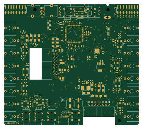 STM32
STM32Plinkyblack hwmidi jacks
121.9 × 109.2 mm261 parts4LMIT221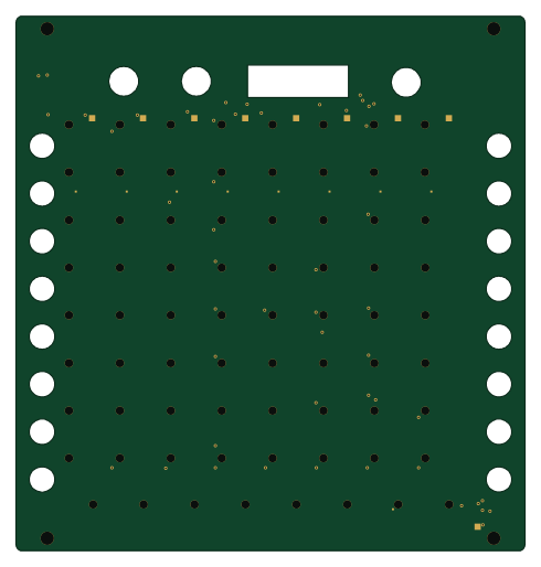
Plinky front osh
121.9 × 128.3 mm76 parts2LMIT221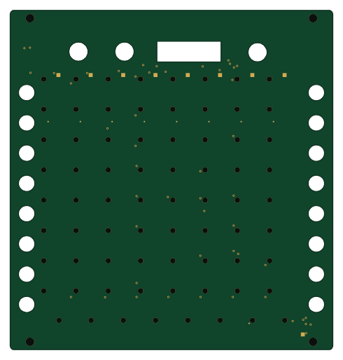
Plinkyblackfront bigholes
121.9 × 128.3 mm76 parts2LMIT221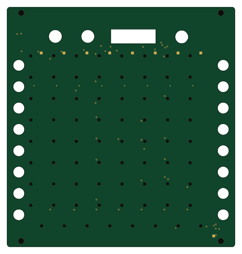
Plinkyblackfront
121.9 × 128.3 mm76 parts2LMIT221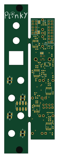
Xyab
43.2 × 128.3 mm68 parts2LMIT221