
Mynd LINE IN Jack


About the Mynd LINE IN Jack PCB
Mynd LINE IN Jack is an open source PCB design by Prototype-Fund-Hardware, published on GitHub. It is a 2-layer board measuring 24.1 × 16.5 mm, with 18 components from 11 distinct parts.
By type, the board carries 4 test points, 2 connectors, 2 microphones, 2 inductors, 2 capacitors and 2 resistors.
From the project
Inofficial hardware repository for the Teufel MYND loudspeaker: https://teufel.de/mynd-107002004
Due to the file size, the STL files were not uploaded. They can be downloaded directly from the Teufel website: https://docs.teufel.de/download/MYND/open_source.zip
The repository for the firmware can be found here: https://github.com/teufelaudio/mynd-firmware
Mynd LINE IN Jack bill of materials (BOM)
18 components, 11 distinct parts.
| Qty | Part | Footprint | Refs |
|---|---|---|---|
| 1 | MH35A080-F05J1BR-C | PJ_MH35A080-F05J1BR-C | J2L |
| 1 | WB200AW-6 | WB200AW_2x3P | P2L |
| 1 | CESD0501CU | DFN2_100X60X50_65 | ESD6L |
| 1 | SM24C | SOT23-123 | ESD7L |
| 2 | — | MARK | MK1J, MK2J |
| 4 | TP12 | TP120 | TP6J, TP11J, TP12J, TP13J |
| 1 | 3.2 | Teufel_ASM_Rev | Teufel_ASM_Label1J |
| 1 | 3.2 | Teufel_PCB_Rev | Teufel_PCB_Label1J |
| 2 | FCM1608KF-601T05 600R | L0603 | FB1L, FB2L |
| 2 | Generic 100pF | C0603X80 | C7L, C8L |
| 2 | Generic 0R | R0603 | R3L, R4L |
Mynd LINE IN Jack design files
The KiCad project lives in the Prototype-Fund-Hardware/MYND-Hardware repository on GitHub; these links point at the commit this page was built from.
Mynd LINE IN Jack: common questions
How big is the Mynd LINE IN Jack PCB?
The Mynd LINE IN Jack measures 24.1 × 16.5 mm, has 2 copper layers and is 1.6 mm thick.
How many components are on the Mynd LINE IN Jack?
18 components, from 11 distinct parts. The full bill of materials is listed on this page.
Where can I download the Mynd LINE IN Jack design files?
From the Prototype-Fund-Hardware/MYND-Hardware repository on GitHub, which has the KiCad layout and the schematic; the links under Design files point to each one.
Can I use the Mynd LINE IN Jack design in my own project?
The repository has no license, so all rights stay with Prototype-Fund-Hardware. Use it as a reference, and ask the author before reusing the design.
More boards in MYND-Hardware
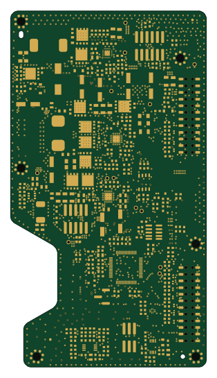 STM32
STM32Mynd Main
75 × 136 mm560 parts4LNo license3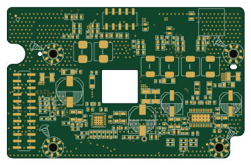
Mynd AMP
90.5 × 57.5 mm158 parts2LNo license3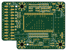
Mynd BT
55 × 41 mm135 parts4LNo license3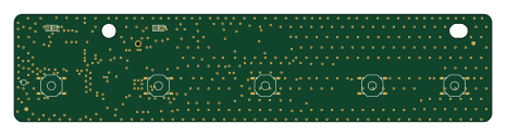
Mynd UI
116 × 26 mm81 parts2LNo license3
Mynd USB JACK
23 × 20.8 mm38 parts2LNo license3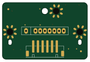
Mynd Baffle
45 × 30 mm17 parts2LNo license3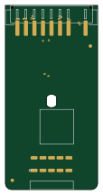
Mynd Conn
27 × 54 mm15 parts2LNo license3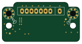
Mynd Batt
41 × 21 mm14 parts2LNo license3