
SNES S-CPU Schematics

About the SNES S-CPU Schematics PCB
SNES S-CPU Schematics is an open source PCB design by rgalland, published on GitHub under the GPL-3.0 license. It is a board, with 8 components from 1 distinct parts.
It belongs with the retro computing designs in this gallery.
From the project
Reverse engineering of the SNES CPU from dies shots
- All cell types have been identified (with the exception of the 65816 section) - All cells have been allocated a 4 letter unique identifier in the SVG file - All cells captured are in Kicad schematics - Schematics rearranged in sections. Only some DMA section still require a few more notes and to be tidied up. - TODO: Adding 65816 as a component (still some unknow external connections .. to me anyway)
SNES S-CPU Schematics bill of materials (BOM)
8 components, 1 distinct parts.
| Qty | Part | Footprint | Refs |
|---|---|---|---|
| 8 | IOBUF_B | JPIO0, JPIO1, JPIO2, JPIO3, JPIO4, JPIO5, JPIO6, JPIO7 |
SNES S-CPU Schematics design files
The KiCad project lives in the rgalland/SNES_S-CPU_Schematics repository on GitHub; these links point at the commit this page was built from.
- SchematicS-CPU_kicad/joypads.kicad_sch
SNES S-CPU Schematics: common questions
How many components are on the SNES S-CPU Schematics?
8 components, from 1 distinct parts. The full bill of materials is listed on this page.
Where can I download the SNES S-CPU Schematics design files?
From the rgalland/SNES_S-CPU_Schematics repository on GitHub, which has the schematic; the links under Design files point to each one.
Can I use the SNES S-CPU Schematics design in my own project?
Yes, under the terms of its GPL-3.0 license, which rgalland chose for the repository.
Similar boards
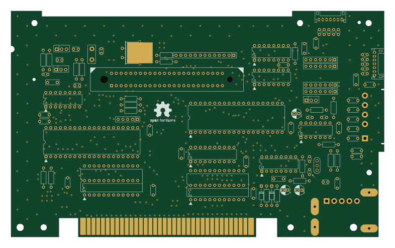
OpenTendo
Redherring32
196.3 × 118.7 mm93 parts2LTAPR-OHL-1.0850
MCL86jr
MicroCoreLabs
56.1 × 57.1 mm66 parts4LNo license532
24pin flex interposer
Wren6991
29 × 32 mm3 parts2LNo license508
Sram dev board
50 × 50 mm12 parts2LNo license508
TRS-80 Color Computer 3
baldengineer
280 × 155.3 mm204 parts2LCC-BY-4.0442
Commodore Plus 4
284.7 × 158.9 mm212 parts2LCC-BY-4.0442