
002.35.20.15.20-001-PCB-LNA

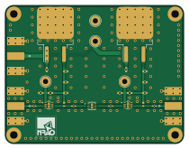
About the 002.35.20.15.20-001-PCB-LNA
002.35.20.15.20-001-PCB-LNA is an open source PCB design by RomiFC, published on GitHub. It is a 4-layer board measuring 52.5 × 40.5 mm, with 30 components from 14 distinct parts.
Other key parts include the PMA2-63LN+, YAT-1A+ and L7805. By type, the board carries 12 capacitors, 5 ICs, 4 test points, 4 resistors, 3 connectors and 2 inductors.
It belongs with the test & measurement designs in this gallery.
From the project
Environmental RFI monitoring system for the NRAO VLA
- Drawing sheets changed from A4 to Letter size. - New stackup table format.
- SMA launch pad widened with ground plane cutout to improve Z-matching. - Mounting holes now correctly part of GND net.
- GCPW cross-section to assembly drawing. - Board characteristics to assembly drawing. - Board dimensioning to assembly drawing. - Test points for DC power as an alternative to SMA. - Test points for Iadj control. - More PTH vias around and directly under RF components. - Layer indicator to top left of assembly drawing.
Main components on the 002.35.20.15.20-001-PCB-LNA
002.35.20.15.20-001-PCB-LNA bill of materials (BOM)
30 components, 14 distinct parts.
| Qty | Part | Footprint | Refs |
|---|---|---|---|
| 2 | PMA2-63LN+ | SON8_PMA2_MNC | U1, U2 |
| 1 | YAT-1A+ | MC1630_MNC | U3 |
| 2 | L7805 | TO-263-2 | U4, U5 |
| 3 | Conn_Coaxial | SMA_Molex_73251-1153_EdgeMount_Horizontal | J1, J2, J3 |
| 2 | TestPoint | TestPoint_Loop_D2.54mm_Drill1.5mm_Beaded | TP1, TP2 |
| 1 | Vin | TestPoint_Loop_D2.54mm_Drill1.5mm_Beaded | TP3 |
| 1 | GND | TestPoint_Loop_D2.54mm_Drill1.5mm_Beaded | TP4 |
| 2 | 56nH | L_0402_1005Metric | L1, L2 |
| 4 | 150pF | C_0402_1005Metric | C1, C4, C5, C8 |
| 2 | 1uF | C_0402_1005Metric | C2, C6 |
| 2 | 100pF | C_0402_1005Metric | C3, C7 |
| 2 | 0.33uF | C_0402_1005Metric | C9, C11 |
| 2 | 0.1uF | C_0402_1005Metric | C10, C12 |
| 4 | 100k | R_0402_1005Metric | R1, R2, R3, R4 |
002.35.20.15.20-001-PCB-LNA design files
The KiCad project lives in the RomiFC/nm-spectrum-monitor repository on GitHub; these links point at the commit this page was built from.
002.35.20.15.20-001-PCB-LNA: common questions
How big is the 002.35.20.15.20-001-PCB-LNA?
The 002.35.20.15.20-001-PCB-LNA measures 52.5 × 40.5 mm, has 4 copper layers and is 1.567 mm thick.
How many components are on the 002.35.20.15.20-001-PCB-LNA?
30 components, from 14 distinct parts. The full bill of materials is listed on this page.
Where can I download the 002.35.20.15.20-001-PCB-LNA design files?
From the RomiFC/nm-spectrum-monitor repository on GitHub, which has the KiCad layout and the schematic; the links under Design files point to each one.
Can I use the 002.35.20.15.20-001-PCB-LNA design in my own project?
The repository has no license, so all rights stay with RomiFC. Use it as a reference, and ask the author before reusing the design.
More boards in nm-spectrum-monitor
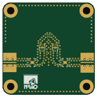
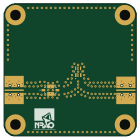
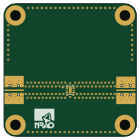
Similar boards
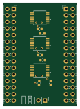
LevelShifter
gusmanb
28.3 × 39.8 mm21 parts2LGPL-3.05.0k
StackLink
52.3 × 10.5 mm5 parts2LGPL-3.05.0k
AnalyzerBoxPCB fork
52.7 × 47.9 mm54 parts4LGPL-3.05.0k
EleLab v2 Bus100
Chrismettal
100 × 100 mm37 parts2LGPL-3.0528
EleLab v2 Bus150
150 × 50 mm37 parts2LGPL-3.0528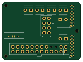
EleLab v2 PowerFeed
68 × 50 mm11 parts2LGPL-3.0528