
EGKeyPCB-routingV2

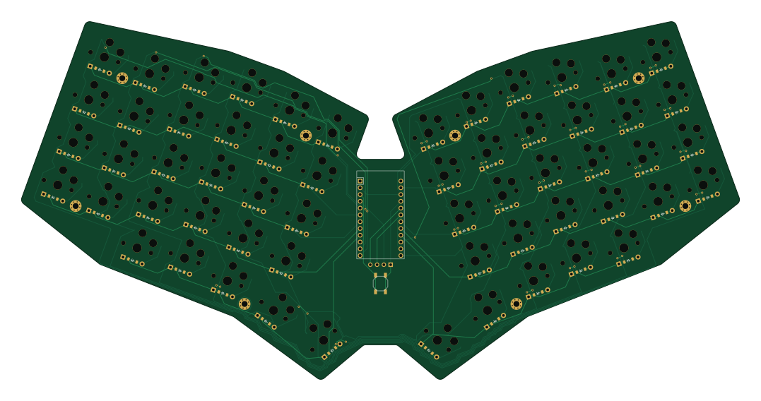
About the EGKeyPCB-routingV2 PCB
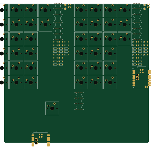
EGKeyPCB-routingV2 is an open source PCB design by Sh4rk-glitch, published on GitHub. It is a 2-layer board measuring 268.9 × 134 mm, with 119 components from 5 distinct parts.
By type, the board carries 58 switches, 58 diodes, 1 IC and 1 LED.
It belongs with the keyboards and displays & leds designs in this gallery.
From the project
A custom ergonomic keyboard PCB design (ErgoKey) using Choc-style hotswap sockets, Promicro controller footprint, and an optional OLED. The repository contains the PCB files, output DXF/gerbers, footprint helpers, and a YAML-based configuration used to generate outlines and placements.
A custom ergonomic keyboard PCB design using Choc-style hotswap sockets, a face-down Promicro footprint, and an optional OLED. This repository contains KiCad board sources, generated gerbers, mechanical DXF outlines, and footprint helper scripts driven by a YAML configuration.
All images are located on my journal, at: https://blueprint.hackclub.com/projects/5019
EGKeyPCB-routingV2 bill of materials (BOM)
119 components, 5 distinct parts — part numbers from the project's BOM.
| Qty | Part | Footprint | Refs |
|---|---|---|---|
| 1 | — | ProMicro | MCU1 |
| 1 | — | SW_TACT_ALPS_SKQGABE010 | B1 |
| 58 | — | PG1350 | S1, S2, S3, S4, S5, S6, S7, S8 +50 |
| 1 | OLED | OLED_headers | OLED1 |
| 58 | — | ComboDiode | D1, D2, D3, D4, D5, D6, D7, D8 +50 |
EGKeyPCB-routingV2 design files
The KiCad project lives in the Sh4rk-glitch/EGKey repository on GitHub; these links point at the commit this page was built from.
EGKeyPCB-routingV2: common questions
How big is the EGKeyPCB-routingV2 PCB?
The EGKeyPCB-routingV2 measures 268.9 × 134 mm, has 2 copper layers and is 1.6 mm thick.
How many components are on the EGKeyPCB-routingV2?
119 components, from 5 distinct parts, with part numbers taken from the project's own BOM. The full bill of materials is listed on this page.
Where can I download the EGKeyPCB-routingV2 design files?
From the Sh4rk-glitch/EGKey repository on GitHub, which has the KiCad layout and the BOM; the links under Design files point to each one.
Can I use the EGKeyPCB-routingV2 design in my own project?
The repository has no license, so all rights stay with Sh4rk-glitch. Use it as a reference, and ask the author before reusing the design.
More boards in EGKey
Similar boards
View base
scottbez1
81.2 × 81.2 mm81 parts2LApache-2.022.2k
BM28B0.6-24DSBreakout
15.2 × 35.6 mm3 parts2LApache-2.022.2k
View screen
35 × 35 mm12 parts2LApache-2.022.2k
LevelShifterBreakout
15.2 × 20.3 mm5 parts2LApache-2.022.2k
Anyon e motherboard
byrantech
133 × 92 mm258 parts6LMIT4.3k
Switch
18.5 × 11.1 mm5 parts2LMIT4.3k