Logic probe

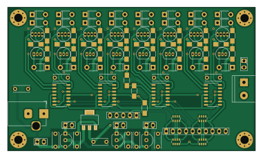
About the Logic probe PCB
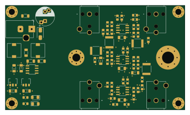
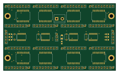
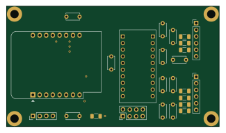
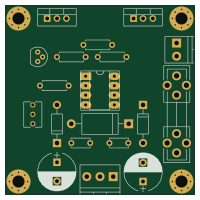
Logic probe is an open source PCB design by sjm42, published on GitHub under the Apache-2.0 license. It is a 2-layer board measuring 95 × 55 mm, with 99 components from 25 distinct parts.
Other key parts include the TLE2426XD, L78L08_SOT89, L79L08_SOT89, OPA1612AXD and LM339. By type, the board carries 31 resistors, 24 diodes, 11 capacitors, 8 ICs, 8 transistors and 8 LEDs.
From the project
Various electronics projects
Main components on the Logic probe
Logic probe bill of materials (BOM)
99 components, 25 distinct parts — part numbers from the project's BOM.
| Qty | Part | Footprint | Refs |
|---|---|---|---|
| 1 | TLE2426XD L78L05 | TO-92_Inline_Wide | U1 |
| 1 | L78L08_SOT89 L78L10 | TO-92_Inline_Wide | U2 |
| 1 | L79L08_SOT89 L78L15 | TO-92_Inline_Wide | U3 |
| 3 | OPA1612AXD LM339 | SOIC-14_3.9x8.7mm_Pitch1.27mm | U4, U5, U6 |
| 1 | LM339 | SOIC-14_3.9x8.7mm_Pitch1.27mm | U7 |
| 1 | AMS1117-3.3 | sot223 | U8 |
| 8 | 2N2222A Central Semiconductor Corp | TO-92_Inline_Narrow_Oval | Q0, Q1, Q2, Q3, Q4, Q5, Q6, Q7 |
| 2 | Conn_01x02_Male | pin_strip_2 | J1, J4 |
| 1 | Barrel_Jack_Switch | BarrelJack_Horizontal | J2 |
| 1 | Conn_01x10_Male | pin_strip_10 | J3 |
| 1 | Screw_Terminal_01x02 | mors_2p | J5 |
| 3 | Jumper | pin_strip_2 | JP1, JP2, JP3 |
| 1 | Conn_01x05_Male | pin_strip_5 | JP4 |
| 8 | LED_RAGB | LED-RGB-THRU | LED0, LED1, LED2, LED3, LED4, LED5, LED6, LED7 |
| 24 | 1N4148 | D_T-1_P5.08mm_Horizontal | D0.1, D0.2, D0.3, D1.1, D1.2, D1.3, D2.1, D2.2 +16 |
| 1 | 10u | C_Disc_D6.0mm_W2.5mm_P5.00mm | C1 |
| 2 | 4.7u | C_Disc_D6.0mm_W2.5mm_P5.00mm | C2, C6 |
| 8 | 1u | C_Disc_D6.0mm_W2.5mm_P5.00mm | C3, C4, C5, C7, C8, C9, C10, C11 |
| 8 | 470 | R_1206_HandSoldering | R0.1, R1.1, R2.1, R3.1, R4.1, R5.1, R6.1, R7.1 |
| 8 | 47k | R_1206_HandSoldering | R0.2, R1.2, R2.2, R3.2, R4.2, R5.2, R6.2, R7.2 |
Show 5 more
| Qty | Part | Footprint | Refs |
|---|---|---|---|
| 8 | 100 | R_1206_HandSoldering | R0.3, R1.3, R2.3, R3.3, R4.3, R5.3, R6.3, R7.3 |
| 1 | 3.3K 7.5k | R_1206_HandSoldering | R1 |
| 1 | 3.3K 10k | R_1206_HandSoldering | R2 |
| 1 | 7.5k | R_1206_HandSoldering | R3 |
| 4 | 470k | R_Array_Concave_4x0603 | RN1, RN2, RN3, RN4 |
Logic probe design files
The KiCad project lives in the sjm42/electronics repository on GitHub; these links point at the commit this page was built from.
Logic probe: common questions
How big is the Logic probe PCB?
The Logic probe measures 95 × 55 mm, has 2 copper layers and is 1.6 mm thick.
How many components are on the Logic probe?
99 components, from 25 distinct parts, with part numbers taken from the project's own BOM. The full bill of materials is listed on this page.
Where can I download the Logic probe design files?
From the sjm42/electronics repository on GitHub, which has the KiCad layout, the schematic and the BOM; the links under Design files point to each one.
Can I use the Logic probe design in my own project?
Yes, under the terms of its Apache-2.0 license, which sjm42 chose for the repository.