
Kicad

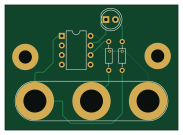
About the Kicad PCB
Kicad is an open source PIC PCB design by suyashsingh, published on GitHub. It is a 2-layer board measuring 45.7 × 33 mm, with 5 components from 5 distinct parts.
Its main chip is the PIC12C508A-ISN, from the PIC family. By type, the board carries 2 resistors, 1 IC, 1 connector and 1 diode.
From the project
Following along with KiCad official tutorial.
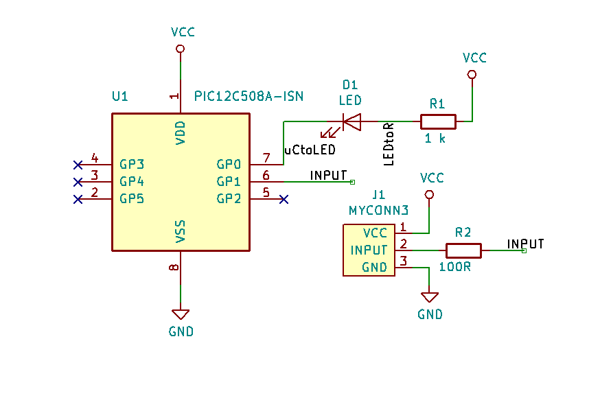
Main components on the Kicad
Kicad bill of materials (BOM)
5 components, 5 distinct parts.
| Qty | Part | Footprint | Refs |
|---|---|---|---|
| 1 | PIC12C508A-ISN | DIP-8_W7.62mm | U1 |
| 1 | MYCONN3 | Banana_Jack_3Pin | J1 |
| 1 | LED | LED_D5.0mm | D1 |
| 1 | 1 k | R_Axial_DIN0204_L3.6mm_D1.6mm_P7.62mm_Horizontal | R1 |
| 1 | 100R | R_Axial_DIN0204_L3.6mm_D1.6mm_P7.62mm_Horizontal | R2 |
Kicad design files
The KiCad project lives in the suyashsingh/kicad repository on GitHub; these links point at the commit this page was built from.
- Layoutkicad-tut.kicad_pcb
Kicad: common questions
What microcontroller does the Kicad use?
The Kicad is built around the PIC12C508A-ISN, from the PIC family.
How big is the Kicad PCB?
The Kicad measures 45.7 × 33 mm, has 2 copper layers and is 1.6 mm thick.
How many components are on the Kicad?
5 components, from 5 distinct parts. The full bill of materials is listed on this page.
Where can I download the Kicad design files?
From the suyashsingh/kicad repository on GitHub, which has the KiCad layout; the links under Design files point to each one.
Can I use the Kicad design in my own project?
The repository has no license, so all rights stay with suyashsingh. Use it as a reference, and ask the author before reusing the design.
Can I test firmware for the Kicad without the hardware?
Yes. HardLabs builds a simulation of the board from its netlist and BOM, so you can run and debug PIC firmware against it before you order a PCB.
Similar boards
 PIC
Pslab hardware
fossasia
99 × 53.3 mm187 parts4LApache-2.01.7k PIC
Lens
ervanalb
80 × 80 mm53 parts4LNo license515 PIC
Micro 8088
skiselev
152.4 × 101.6 mm71 partsGPL-3.0414 PIC
GB-CARTPP-DIY
Gekkio
100 × 100 mm22 parts2LCC-BY-4.0379 PIC
GB-LIVE32
51.4 × 61 mm46 parts4LCC-BY-4.0379 PIC
GB-CART256K-A
51.4 × 61 mm17 parts2LCC-BY-4.0379