
DEV-G2-NANO

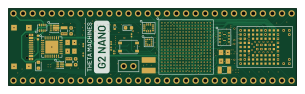
About the DEV-G2-NANO PCB
DEV-G2-NANO is an open source NXP PCB design by theta-machines, published on GitHub under the CERN-OHL-P-2.0 license. It is a 6-layer board measuring 76.2 × 20.3 mm, with 140 components from 38 distinct parts.
Its main chip is the MIMXRT1171DVMAB, from the NXP family. Other key parts include the MAYA-W166-00B, LSM6DSV, LIS2MDL, RTMC-G2-4IQ48 and W25Q64JWUUIQ. By type, the board carries 80 capacitors, 32 resistors, 10 ICs, 5 connectors, 5 inductors and 4 crystals.
It belongs with the sensors and audio designs in this gallery.
From the project
The G2 Nano is powered by a record-breaking 1 GHz Arm Cortex-M7 processor, combining the performance of an application processor with real-time determinism. Purpose-built for robotics R&D, the board integrates dual-band Wi-Fi, an inertial measurement unit, and an on-board closed-
The G2 Nano is powered by a record-breaking 1 GHz Arm Cortex-M7 processor, combining the performance of an application processor with real-time determinism. Purpose-built for robotics R&D, the board integrates dual-band Wi-Fi, an inertial measurement unit, and an on-board closed-loop motion controller.
The KiCad project is contained within the kicad/ directory and can be opened via the kicad/DEV-G2-NANO.kicadpro file.
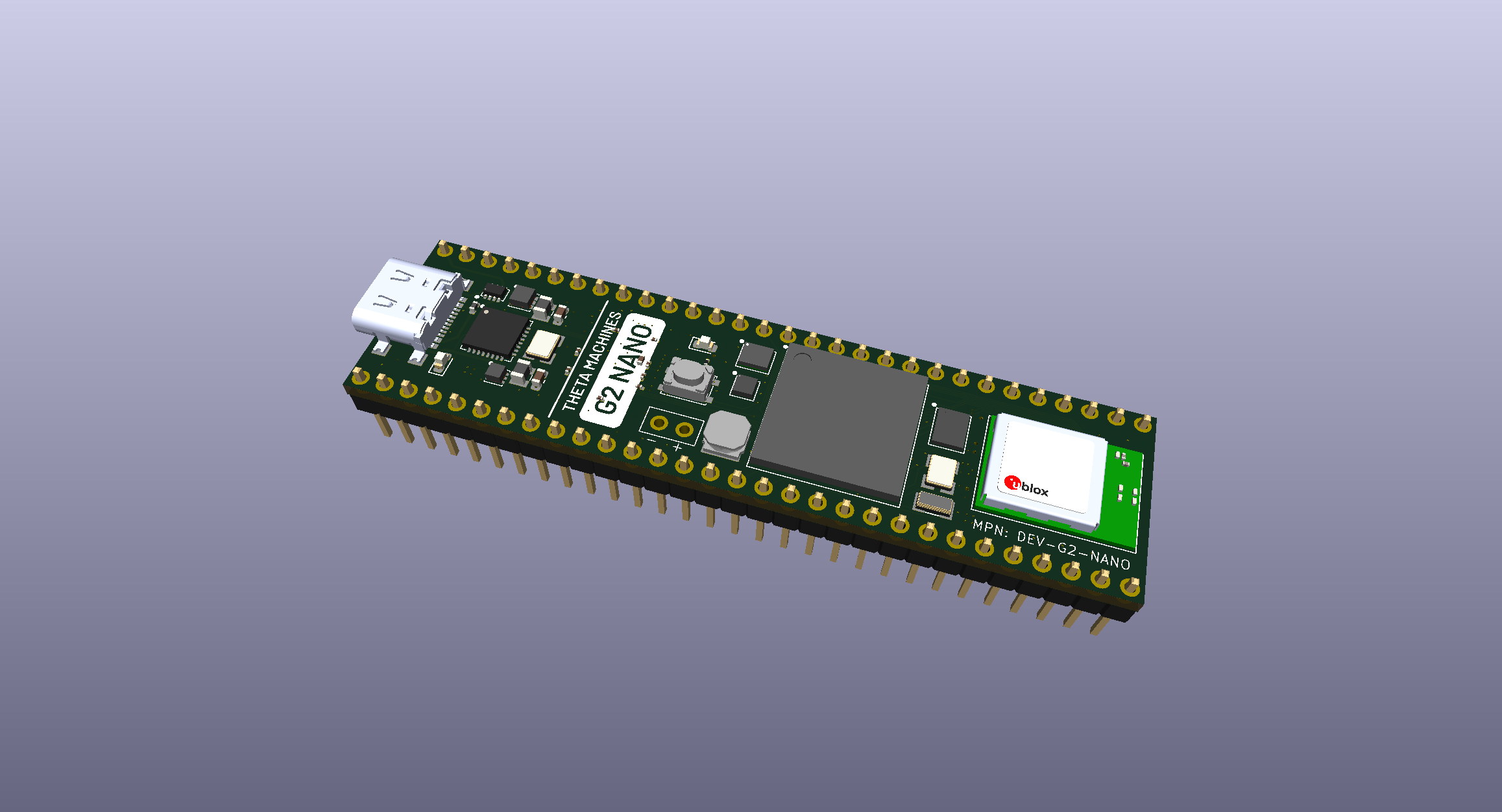
Main components on the DEV-G2-NANO
DEV-G2-NANO bill of materials (BOM)
140 components, 38 distinct parts.
| Qty | Part | Footprint | Refs |
|---|---|---|---|
| 1 | MIMXRT1171DVMAB | MIMXRT1171DVMAB | U1 |
| 1 | MAYA-W166-00B | MAYA-W166-00B | U2 |
| 1 | LSM6DSV | LSM6DSV | U3 |
| 1 | LIS2MDL | LIS2MDL | U4 |
| 1 | RTMC-G2-4IQ48 | RTMC-G2-4IQ48 | U5 |
| 1 | W25Q64JWUUIQ | W25Q64JWUUIQ | U6 |
| 1 | MKL26Z128VFM4 | MKL26Z128VFM4 | U7 |
| 1 | LM66200 | LM66200 | U8 |
| 1 | TPS62086 | TPS62086 | U9 |
| 1 | TPS62825 | TPS62825 | U10 |
| 1 | 8MHz | Crystal-4-Pin | Y1 |
| 1 | 16MHz | Crystal-4-Pin | Y2 |
| 1 | 24MHz | Crystal-4-Pin | Y3 |
| 1 | 32.768kHz | Crystal-2-Pin | Y4 |
| 1 | Lower Bank | Header-1x30 | J1 |
| 1 | Upper Bank | Header-1x30 | J2 |
| 1 | USB C | UJ20-C-H-G-SMT-5-P16 | J3 |
| 1 | HIC SWD | TestPoints-3 | J4 |
| 1 | RTC Battery | Header-1x02 | J5 |
| 1 | PTS815 | PTS815 | SW1 |
Show 18 more
| Qty | Part | Footprint | Refs |
|---|---|---|---|
| 2 | RED | LED_0603_1608Metric | D1, D3 |
| 1 | BAT54C | BAT54C | D2 |
| 1 | 120Ω | L_0402_1005Metric | FB1 |
| 1 | 10μH | L_1008_2520Metric | L1 |
| 1 | 4.7μH | SDCL1V4018 | L2 |
| 2 | 470nH | L_0806 | L3, L4 |
| 26 | 100nF | C_0201_0603Metric | C1, C2, C3, C7, C8, C11, C12, C13 +18 |
| 10 | 10μF | C_0402_1005Metric | C4, C5, C6, C9, C10, C15, C17, C20 +2 |
| 2 | 220nF | C_0201_0603Metric | C16, C67 |
| 8 | 15pF | C_0402_1005Metric | C27, C28, C35, C36, C45, C46, C52, C53 |
| 21 | 2.2μF | C_0201_0603Metric | C30, C33, C37, C40, C42, C43, C48, C55 +13 |
| 6 | 1μF | C_0201_0603Metric | C38, C49, C50, C58, C59, C78 |
| 4 | 22μF | C_0603_1608Metric | C41, C56, C77, C80 |
| 3 | 4.7μF | C_0402_1005Metric | C44, C66, C79 |
| 27 | 10kΩ | R_0201_0603Metric | R1, R3, R4, R5, R6, R7, R8, R9 +19 |
| 1 | 2.2kΩ | R_0201_0603Metric | R2 |
| 1 | 17.8kΩ | R_0201_0603Metric | R12 |
| 3 | 5.1kΩ | R_0201_0603Metric | R16, R19, R31 |
DEV-G2-NANO design files
The KiCad project lives in the theta-machines/DEV-G2-NANO repository on GitHub; these links point at the commit this page was built from.
- Layoutkicad/DEV-G2-NANO.kicad_pcb
- Schematickicad/DEV-G2-NANO.kicad_sch
DEV-G2-NANO: common questions
What microcontroller does the DEV-G2-NANO use?
The DEV-G2-NANO is built around the MIMXRT1171DVMAB, from the NXP family.
How big is the DEV-G2-NANO PCB?
The DEV-G2-NANO measures 76.2 × 20.3 mm, has 6 copper layers and is 1.5584 mm thick.
How many components are on the DEV-G2-NANO?
140 components, from 38 distinct parts. The full bill of materials is listed on this page.
Where can I download the DEV-G2-NANO design files?
From the theta-machines/DEV-G2-NANO repository on GitHub, which has the KiCad layout and the schematic; the links under Design files point to each one.
Can I use the DEV-G2-NANO design in my own project?
Yes, under the terms of its CERN-OHL-P-2.0 license, which theta-machines chose for the repository.
Can I test firmware for the DEV-G2-NANO without the hardware?
Yes. HardLabs builds a simulation of the board from its netlist and BOM, so you can run and debug NXP firmware against it before you order a PCB.
Similar boards
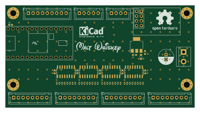 NXP
NXP32Bit shift register
MaltWhiskey
100 × 54 mm56 parts4LNo license763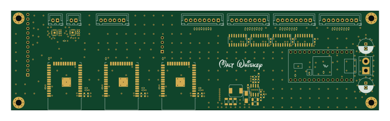 NXP
NXPMega-Cube-Board
200 × 54 mm100 parts4LNo license763 NXP
NXPMCL64
MicroCoreLabs
39.3 × 61.8 mm9 parts4LNo license532 NXP
NXPROM Emulator
21.5 × 37.1 mm5 parts2LNo license532 NXP
NXPMCLZ8
37.1 × 61.5 mm6 parts4LNo license532 NXP
NXPXTMAX
81 × 46 mm14 parts4LNo license532