
Elektronica2-Labo-Opstelling

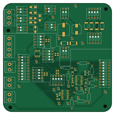
About the Elektronica2-Labo-Opstelling PCB
Elektronica2-Labo-Opstelling is an open source PCB design by TiebeDeclercq, published on GitHub under the MIT license. It is a 2-layer board measuring 100 × 100 mm, with 82 components from 28 distinct parts.
Other key parts include the LM741 and TL074. By type, the board carries 22 connectors, 18 resistors, 15 switches, 12 diodes, 4 capacitors and 3 ICs.
From the project
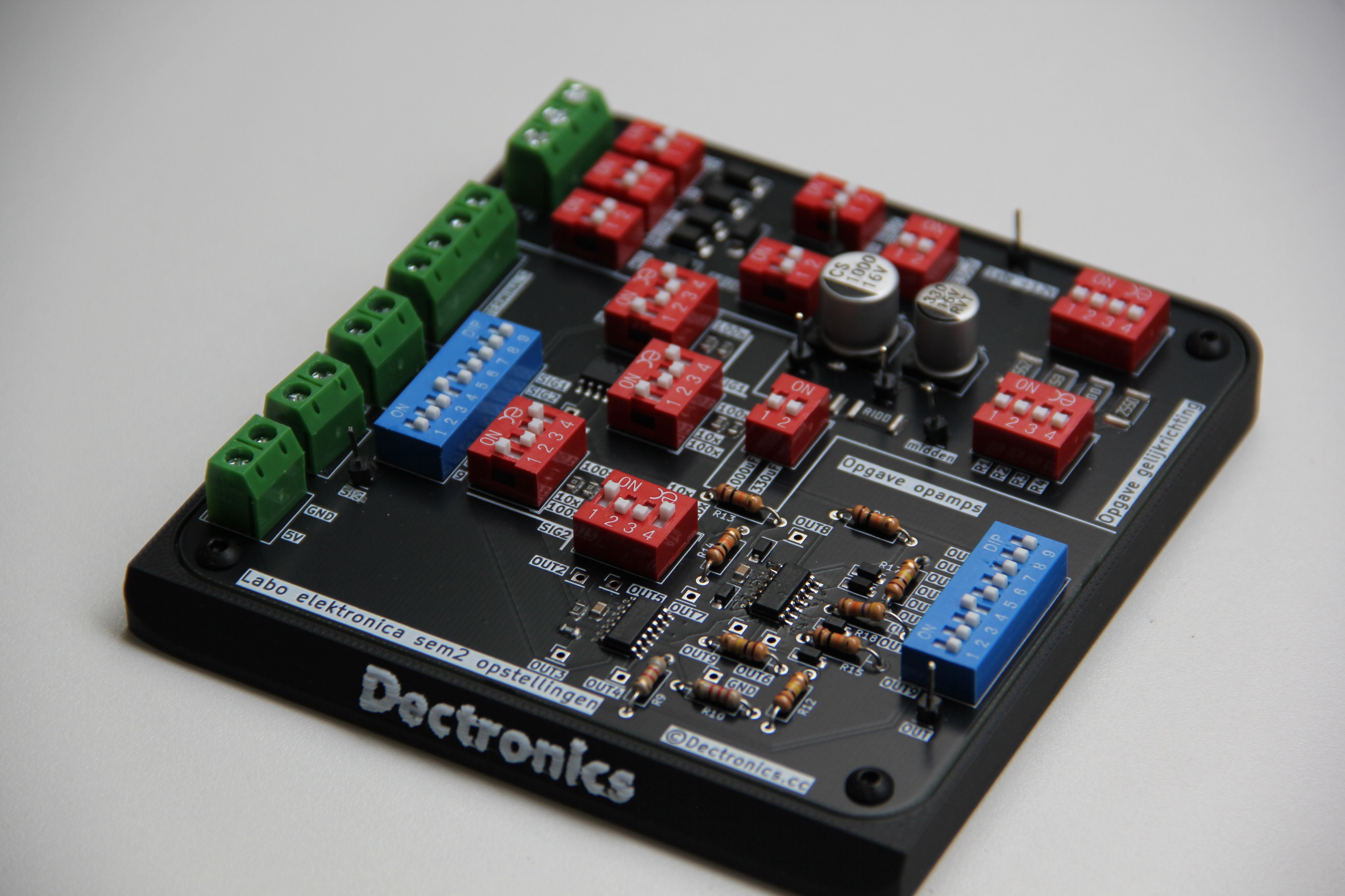
Complete printplaat met alle schakelingen van zowel gelijkrichting als opamps (Vives kortrijk)
Complete printplaat met alle schakelingen van zowel gelijkrichting als opamps @Vives kortrijk Met een printbare voet voor betere stabiliteit en geen kortsluiting te krijgen. Op deze voet wordt er gewerkt met heated inserts (M3) voor het monteren van de print.
Voor het solderen kan je gebruikmaken van de meegeleverde BOM file, alle componenten zijn 0805 buiten sommige TH componenten (omdat deze eigen keuze zijn en makkelijk te verangen moeten zijn)
Main components on the Elektronica2-Labo-Opstelling
Elektronica2-Labo-Opstelling bill of materials (BOM)
82 components, 28 distinct parts.
| Qty | Part | Footprint | Refs |
|---|---|---|---|
| 1 | LM741 | SOIC-8_3.9x4.9mm_P1.27mm | U1 |
| 2 | TL074 | SOIC-14_3.9x8.7mm_P1.27mm | U2, U3 |
| 1 | Screw_Terminal_01x03 | TerminalBlock_Phoenix_MKDS-1,5-3_1x03_P5.00mm_Horizontal | J1 |
| 3 | Screw_Terminal_01x02 | TerminalBlock_Phoenix_MKDS-1,5-2_1x02_P5.00mm_Horizontal | J2, J4, J22 |
| 1 | Screw_Terminal_01x04 | TerminalBlock_Phoenix_MKDS-1,5-4-5.08_1x04_P5.08mm_Horizontal | J3 |
| 17 | Conn_01x01_Pin | PinHeader_1x01_P2.54mm_Vertical | J5, J6, J7, J8, J9, J10, J11, J12 +9 |
| 2 | 10k | R_0805_2012Metric | Rf1, Rf4 |
| 2 | 100k | R_0805_2012Metric | Rf2, Rf3 |
| 2 | 1k | R_0805_2012Metric | Ri1, Ri3 |
| 2 | 100 | R_0805_2012Metric | Ri2, Ri4 |
| 6 | SW_DIP_x04 | SW_DIP_SPSTx04_Slide_9.78x12.34mm_W7.62mm_P2.54mm | SW1, SW2, SW10, SW11, SW12, SW13 |
| 7 | SW_DIP_x02 | SW_DIP_SPSTx02_Slide_9.78x7.26mm_W7.62mm_P2.54mm | SW3, SW4, SW5, SW6, SW7, SW8, SW9 |
| 2 | SW_DIP_x09 | SW_DIP_SPSTx09_Slide_9.78x25.04mm_W7.62mm_P2.54mm | SW14, SW15 |
| 6 | US1M | D_SMA | D1, D2, D7, D8, D9, D10 |
| 6 | D_Zener | D_SOD-123 | D3, D4, D5, D6, D11, D12 |
| 1 | 1000uF | CP_Elec_10x10.5 | C1 |
| 1 | 330uF | CP_Elec_8x10 | C2 |
| 2 | 100nF | C_0805_2012Metric | C3, C4 |
| 1 | 25kΩ, 1W | R_2512_6332Metric | R1 |
| 1 | 14kΩ, 1W | R_2512_6332Metric | R2 |
Show 8 more
| Qty | Part | Footprint | Refs |
|---|---|---|---|
| 1 | 2,5kΩ, 1W | R_2512_6332Metric | R3 |
| 1 | 55Ω, 1W | R_2512_6332Metric | R4 |
| 2 | 0,1Ω, 1W | R_2512_6332Metric | R5, R6 |
| 1 | 1k | R_0805_2012Metric | R7 |
| 1 | 99k | R_0805_2012Metric | R8 |
| 1 | 8k | R_Axial_DIN0207_L6.3mm_D2.5mm_P10.16mm_Horizontal | R9 |
| 1 | 2k | R_Axial_DIN0207_L6.3mm_D2.5mm_P10.16mm_Horizontal | R10 |
| 8 | R | R_Axial_DIN0207_L6.3mm_D2.5mm_P10.16mm_Horizontal | R11, R12, R13, R14, R15, R16, R17, R18 |
Elektronica2-Labo-Opstelling design files
The KiCad project lives in the TiebeDeclercq/Elektronica2-Labo-Opstelling repository on GitHub; these links point at the commit this page was built from.
Elektronica2-Labo-Opstelling: common questions
How big is the Elektronica2-Labo-Opstelling PCB?
The Elektronica2-Labo-Opstelling measures 100 × 100 mm, has 2 copper layers and is 1.6 mm thick.
How many components are on the Elektronica2-Labo-Opstelling?
82 components, from 28 distinct parts. The full bill of materials is listed on this page.
Where can I download the Elektronica2-Labo-Opstelling design files?
From the TiebeDeclercq/Elektronica2-Labo-Opstelling repository on GitHub, which has the KiCad layout and the schematic; the links under Design files point to each one.
Can I use the Elektronica2-Labo-Opstelling design in my own project?
Yes, under the terms of its MIT license, which TiebeDeclercq chose for the repository.