
SAP-Plus Backplane

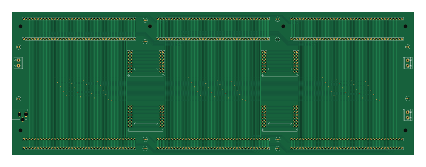
About the SAP-Plus Backplane PCB
SAP-Plus Backplane is an open source PCB design by TomNisbet, published on GitHub under the MIT license. It is a 2-layer board measuring 360 × 128 mm, with 36 components from 5 distinct parts.
By type, the board carries 24 connectors and 12 capacitors.
From the project
Simple As Possible (SAP) 8-bit computer with a modular PCB design
Add barrel connector for power in Rotate C1, C2, C8 for consistent orientation
SAP-Plus Backplane bill of materials (BOM)
36 components, 5 distinct parts.
| Qty | Part | Footprint | Refs |
|---|---|---|---|
| 12 | Bus | PinSocket_1x40_P2.54mm_Vertical | J1, J2, J3, J4, J5, J6, J7, J8 +4 |
| 8 | Conn_02x08 | PinSocket_2x08_P2.54mm_Vertical | J13, J14, J15, J16, J17, J18, J19, J20 |
| 3 | 5V POWER | TerminalBlock_RND_205-00012_1x02_P5.00mm_Horizontal | J21, J22, J23 |
| 1 | 5V POWER IN | BarrelJack_Wuerth_6941xx301002 | J24 |
| 12 | 10uF | C_Radial_D4.0mm_H5.0mm_P1.50mm | C1, C2, C3, C4, C5, C6, C7, C8 +4 |
SAP-Plus Backplane design files
The KiCad project lives in the TomNisbet/sap-plus repository on GitHub; these links point at the commit this page was built from.
SAP-Plus Backplane: common questions
How big is the SAP-Plus Backplane PCB?
The SAP-Plus Backplane measures 360 × 128 mm, has 2 copper layers and is 1.6 mm thick.
How many components are on the SAP-Plus Backplane?
36 components, from 5 distinct parts. The full bill of materials is listed on this page.
Where can I download the SAP-Plus Backplane design files?
From the TomNisbet/sap-plus repository on GitHub, which has the KiCad layout and the schematic; the links under Design files point to each one.
Can I use the SAP-Plus Backplane design in my own project?
Yes, under the terms of its MIT license, which TomNisbet chose for the repository.
More boards in sap-plus
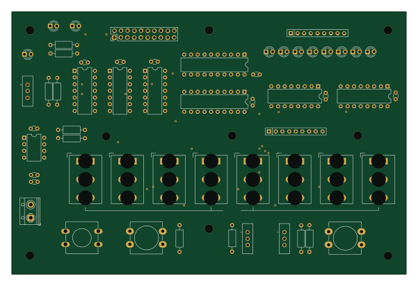
SAP-Plus Memory Loader
150 × 100 mm57 parts2LMIT10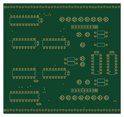
SAP-Plus Program Counter and Stack Pointer
102 × 96 mm50 parts2LMIT10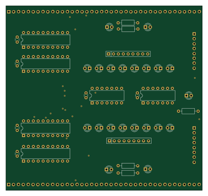
SAP-Plus A and B Registers
102 × 96 mm44 parts2LMIT10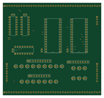
SAP-Plus Microcode
102 × 96 mm40 parts2LMIT10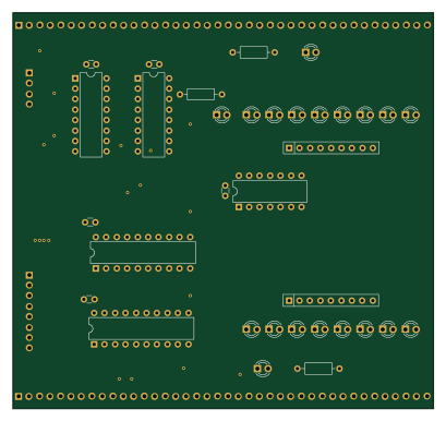
SAP-Plus Instruction Register and Step Counter
102 × 96 mm38 parts2LMIT10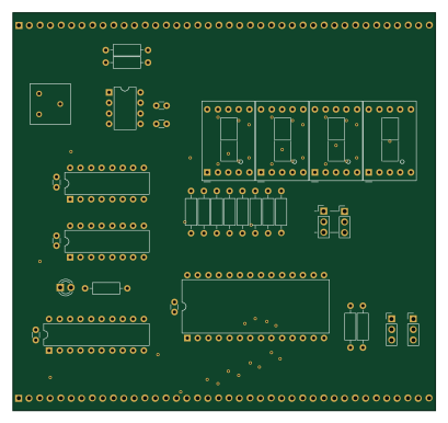
SAP-Plus Output Register
102 × 96 mm36 parts2LMIT10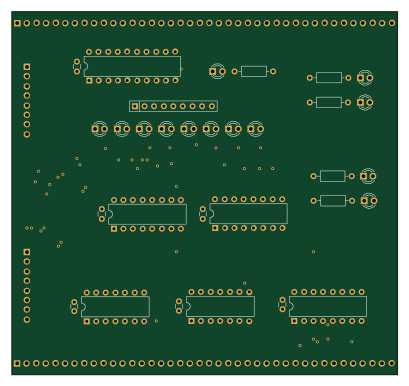
SAP-Plus ALU
102 × 96 mm35 parts2LMIT10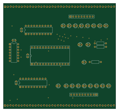
SAP-Plus RAM and MAR
102 × 96 mm35 parts2LMIT10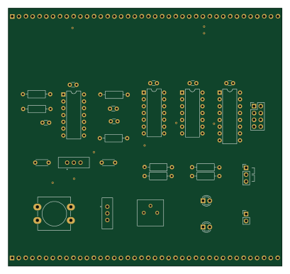
SAP-Plus System Clock
102 × 96 mm32 parts2LMIT10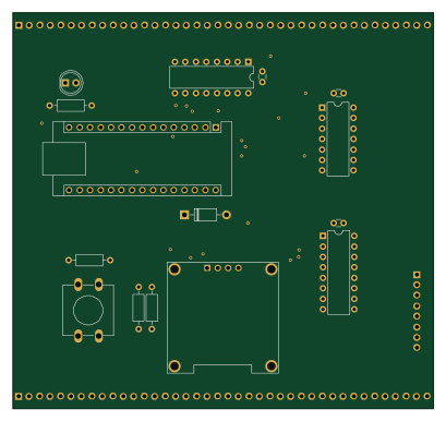 AVR/Arduino
SAP-Plus Loader / Debugger
102 × 96 mm18 parts2LMIT10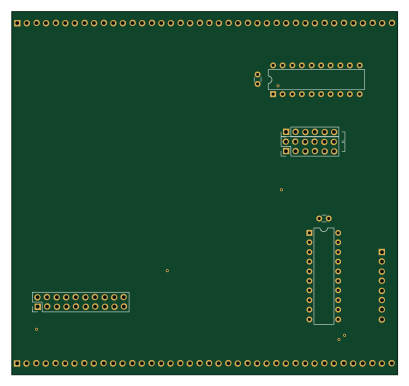
SAP-Plus Memory Loader Interface
102 × 96 mm10 parts2LMIT10