
SAP-Plus System Clock

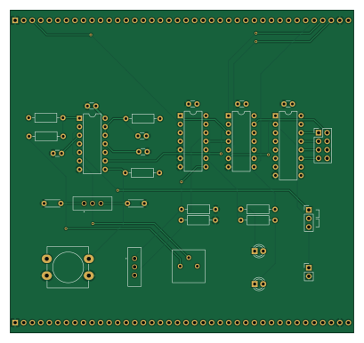
About the SAP-Plus System Clock PCB
SAP-Plus System Clock is an open source PCB design by TomNisbet, published on GitHub under the MIT license. It is a 2-layer board measuring 102 × 96 mm, with 32 components from 22 distinct parts.
Other key parts include the NE556, 74LS02, 74LS27 and 74LS161. By type, the board carries 9 capacitors, 8 resistors, 5 connectors, 4 ICs, 3 switches and 2 diodes.
From the project
Simple As Possible (SAP) 8-bit computer with a modular PCB design
Add range switch to select from two capacitor values for the astable clock Add 4-bit counter clock divider to fix clock reset problem and allow more astable clock frequency ranges Change astable potentiometer from 1M to 100K - allows for finer control while range switch and divider still allow wide range for frequencies RUN/STOP, RST, and LD_ACT signals now hold the divider clock in reset rather than just gating the astable clock, ensuring that the clock always starts low and the first transition is a rising edge
Main components on the SAP-Plus System Clock
SAP-Plus System Clock bill of materials (BOM)
32 components, 22 distinct parts.
| Qty | Part | Footprint | Refs |
|---|---|---|---|
| 1 | NE556 | DIP-14_W7.62mm | U1 |
| 1 | 74LS02 | DIP-14_W7.62mm | U2 |
| 1 | 74LS27 | DIP-14_W7.62mm | U3 |
| 1 | 74LS161 | DIP-16_W7.62mm | U4 |
| 2 | Bus | PinHeader_1x40_P2.54mm_Vertical | J1, J2 |
| 1 | Conn_02x04_Odd_Even | PinHeader_2x04_P2.54mm_Vertical | J3 |
| 1 | CLOCK SELECT | PinHeader_1x03_P2.54mm_Vertical | J4 |
| 1 | EXTERNAL CLOCK IN | PinHeader_1x02_P2.54mm_Vertical | J5 |
| 1 | 100K | Potentiometer_Bourns_3386P_Vertical | RV1 |
| 1 | STOP | SW_EG1218 | SW1 |
| 1 | PULSE | SW_PUSH-12mm_Wuerth-430476085716 | SW2 |
| 1 | SPDT | SW_EG1218 | SW3 |
| 1 | STOP | LED_D3.0mm | D1 |
| 1 | CLOCK | LED_D3.0mm | D2 |
| 5 | 0.1uF | C_Disc_D3.0mm_W1.6mm_P2.50mm | C1, C2, C3, C4, C7 |
| 2 | 0.01uF | C_Disc_D3.0mm_W1.6mm_P2.50mm | C5, C6 |
| 1 | 0.047uF | C_Disc_D4.3mm_W1.9mm_P5.00mm | C8 |
| 1 | 1.5uF | C_Disc_D4.3mm_W1.9mm_P5.00mm | C9 |
| 5 | 1K | R_Axial_DIN0207_L6.3mm_D2.5mm_P10.16mm_Horizontal | R1, R2, R3, R4, R7 |
| 1 | R-RED | R_Axial_DIN0207_L6.3mm_D2.5mm_P10.16mm_Horizontal | R5 |
Show 2 more
| Qty | Part | Footprint | Refs |
|---|---|---|---|
| 1 | R-BLUE | R_Axial_DIN0207_L6.3mm_D2.5mm_P10.16mm_Horizontal | R6 |
| 1 | 1M | R_Axial_DIN0207_L6.3mm_D2.5mm_P10.16mm_Horizontal | R8 |
SAP-Plus System Clock design files
The KiCad project lives in the TomNisbet/sap-plus repository on GitHub; these links point at the commit this page was built from.
SAP-Plus System Clock: common questions
How big is the SAP-Plus System Clock PCB?
The SAP-Plus System Clock measures 102 × 96 mm, has 2 copper layers and is 1.6 mm thick.
How many components are on the SAP-Plus System Clock?
32 components, from 22 distinct parts. The full bill of materials is listed on this page.
Where can I download the SAP-Plus System Clock design files?
From the TomNisbet/sap-plus repository on GitHub, which has the KiCad layout and the schematic; the links under Design files point to each one.
Can I use the SAP-Plus System Clock design in my own project?
Yes, under the terms of its MIT license, which TomNisbet chose for the repository.
More boards in sap-plus
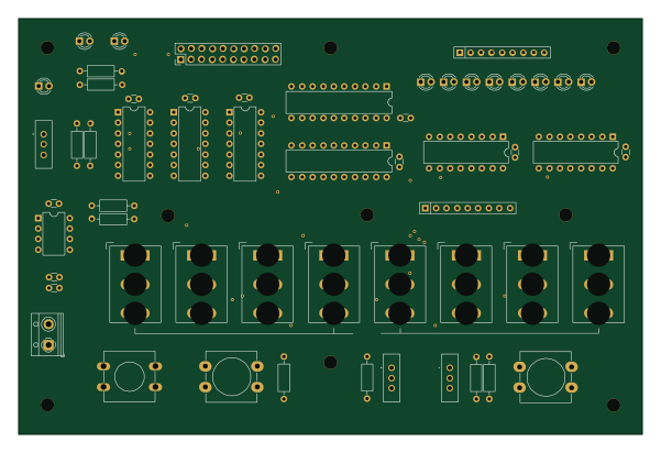
SAP-Plus Memory Loader
150 × 100 mm57 parts2LMIT10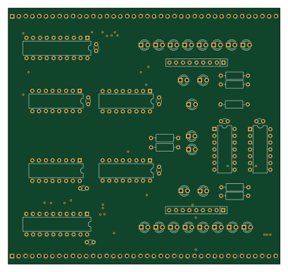
SAP-Plus Program Counter and Stack Pointer
102 × 96 mm50 parts2LMIT10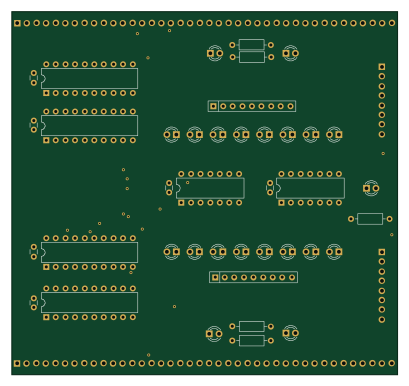
SAP-Plus A and B Registers
102 × 96 mm44 parts2LMIT10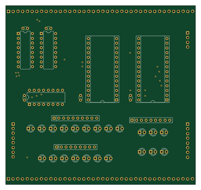
SAP-Plus Microcode
102 × 96 mm40 parts2LMIT10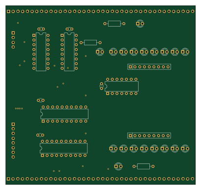
SAP-Plus Instruction Register and Step Counter
102 × 96 mm38 parts2LMIT10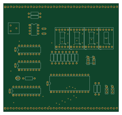
SAP-Plus Output Register
102 × 96 mm36 parts2LMIT10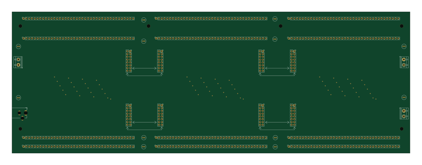
SAP-Plus Backplane
360 × 128 mm36 parts2LMIT10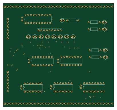
SAP-Plus ALU
102 × 96 mm35 parts2LMIT10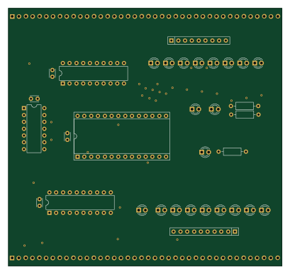
SAP-Plus RAM and MAR
102 × 96 mm35 parts2LMIT10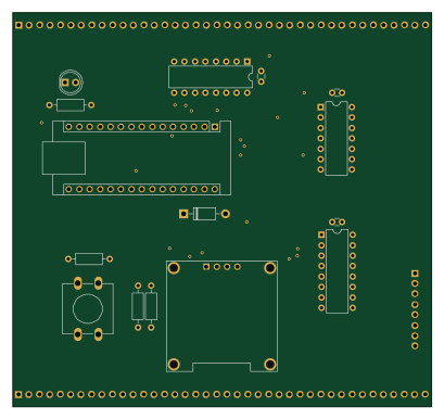 AVR/Arduino
SAP-Plus Loader / Debugger
102 × 96 mm18 parts2LMIT10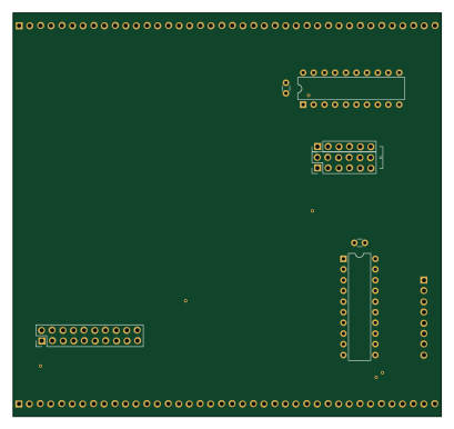
SAP-Plus Memory Loader Interface
102 × 96 mm10 parts2LMIT10