
Sub sys pdu

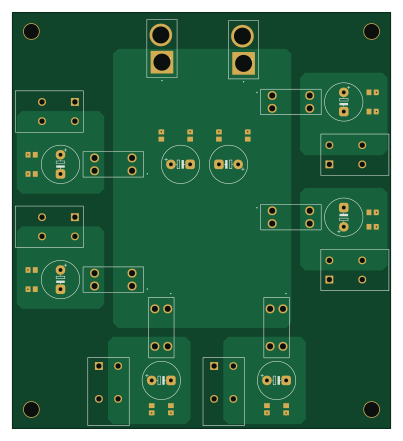
About the Sub sys pdu PCB
Sub sys pdu is an open source PCB design by UofA-SPEAR, published on GitHub. It is a 2-layer board measuring 100 × 110 mm, with 38 components from 5 distinct parts.
By type, the board carries 24 capacitors, 6 connectors, 6 fuses and 2 transistors.
From the project
A place for SPEAR PCBs
Central repository to hold PCB designs for SPEAR.
All board documentation shall be held in the Wiki..
If you plan on contributing to the PCB designs, first, you need to go through this list:
1. Sign up for github, and fill out the new member form (contact the current team lead for this). 2. Follow the GitHub Guides, specifically: - "Hello World" - "Understanding the GitHub flow." - "Documenting your projects on GitHub" 3. Follow the Onboarding Task.
Sub sys pdu bill of materials (BOM)
38 components, 5 distinct parts.
| Qty | Part | Footprint | Refs |
|---|---|---|---|
| 2 | XT60_YELLOW | AMASS_XT60PB-M | Q1, Q3 |
| 6 | 1017503 | 1017503 | J1, J2, J3, J4, J5, J6 |
| 6 | 3568 | FUSE_3568 | F1, F2, F3, F4, F5, F6 |
| 16 | 100nF | C0805 | C1, C3, C4, C6, C7, C9, C10, C12 +8 |
| 8 | 100uf | E5-10,5 | C2, C5, C8, C11, C14, C17, C20, C23 |
Sub sys pdu design files
The KiCad project lives in the UofA-SPEAR/pcb_designs repository on GitHub; these links point at the commit this page was built from.
Sub sys pdu: common questions
How big is the Sub sys pdu PCB?
The Sub sys pdu measures 100 × 110 mm, has 2 copper layers and is 1.6 mm thick.
How many components are on the Sub sys pdu?
38 components, from 5 distinct parts. The full bill of materials is listed on this page.
Where can I download the Sub sys pdu design files?
From the UofA-SPEAR/pcb_designs repository on GitHub, which has the KiCad layout and the schematic; the links under Design files point to each one.
Can I use the Sub sys pdu design in my own project?
The repository has no license, so all rights stay with UofA-SPEAR. Use it as a reference, and ask the author before reusing the design.
More boards in pcb_designs
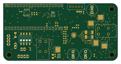
Arm controller single v1.1
100 × 50 mm51 parts2LNo license3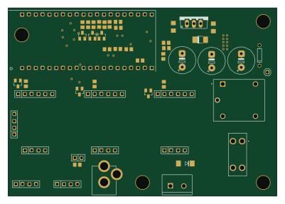
Comp PDU
100 × 70 mm50 parts2LNo license3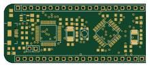 STM32
STM32Green Pill stlink
55 × 23 mm42 parts2LNo license3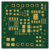
Buck module 5v
25 × 25 mm28 parts2LNo license3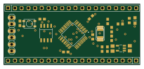 STM32
STM32Speedy barebone
51.2 × 23 mm23 parts2LNo license3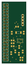
IMU
21.3 × 53.7 mm17 parts2LNo license3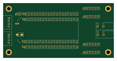
Speedy Breakout Board
100 × 50 mm9 parts2LNo license3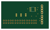
Communication hub
51.7 × 30.5 mm7 parts2LNo license3
As5600 adapter
16 × 16 mm6 parts2LNo license3
Canbus basic
20 × 4 mm5 parts2LNo license3